Self-consistent Electro-thermal Simulation of AlGaN/GaN HEMTs for Reliability Prediction

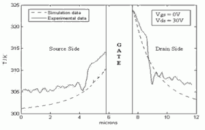
Figure 1: Simulation and thermo-reflectance measurements of the surface temperature along the channel.
During the last few years, AlGaN/GaN high-electron-mobility transistors (HEMTs) have been intensively studied for high-frequency high-power applications. In spite of this great interest, device reliability is still an important challenge for the wide deployment of AlGaN/GaN HEMT technology. Since AlGaN and GaN are both piezoelectric materials, most published work has focused on the role of the inverse piezoelectric effect induced by the electric field [1] [2]; however, lattice heating also changes the mechanical properties of HEMTs, and its effect on device reliability is also important. In this project, we have developed the first fully-coupled electro-thermo-mechanical simulation of AlGaN/GaN HEMTs to study the reliability of these devices as a function of bias voltage and operating temperature. In addition, we have compared the numerical results of our simulations with high-resolution thermo-reflectance measurements [3], obtaining excellent agreement.

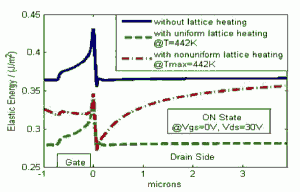
Figure 2: Elastic energy of the Al0.26Ga0.74N layer along the channel as a function of different thermal/heating conditions. The device is biased in the ON state (Vgs= 0V, Vds= 30V).
Figure 1 compares the simulated surface temperature along the channel of an AlGaN/GaN transistor with the experimental data obtained from thermo-reflectance measurements. Excellent agreement was found, especially on the drain side. The mechanical stress and the elastic energy in AlGaN/GaN transistors have been calculated using MATLAB, using as input data the electric field and lattice temperature distribution simulated by Silvaco Atlas. Figure 2 shows the lateral elastic energy in the Al0.26Ga0.74N layer for different self-heating conditions when being biased in the ON state. According to these results, the uniform lattice heating decreases the elastic energy in the Al0.26Ga0.74N layer by ~20% (solid and dash lines). Moreover, if the device operates in the ON state under perfect heat dissipation conditions (dash-dot line), the elastic energy will rise up to ~20% on the drain side of the device. In all the analyzed cases, the elastic energy peaks under the drain edge of the gate, which supports the mechanism of the defect and crack formation in that area.
References
- B. Jogai, J. D. Albrecht, and E. Pan, J. Appl. Phys. 94, 6566 (2003); 94, 3984 (2003). [↩]
- J. Joh, F. Gao, T. Palacios, and J.A. del Alamo, Reliability of Compound Semiconductors Workshop 2009 (ROCS 2009), Greensboro, NC, October 11, 2009, pp. 3-5. [↩]
- P. Mayer, D. Lueerssen, R.J. Ram, and J. Hudgings, “Theoretical and experimental investigation of the resolution and dynamic range of CCD-based thermoreflectance imaging,” Journal of the Optical Society of America A, 24, 1156-1163 (2007). [↩]