Scanning-beam Interference Lithography

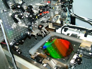
Figure 1: Photograph of the Nanoruler lithography and metrology system built by MIT students. This unique tool is the most precise grating patterning and metrology system in the world.
Traditional methods of fabricating gratings, such as diamond-tip ruling, electron- and laser-beam scanning, or holography, are generally very slow and expensive and result in gratings with poor control of phase and period. More complex periodic patterns, such as gratings with chirped or curved, lines, or 2D and 3D photonic patterns, are even more difficult to pattern. This research program seeks to develop advanced interference lithography tools and techniques to enable the rapid patterning of general periodic patterns with much lower cost and higher fidelity than current technology.

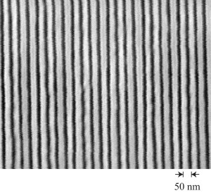
Figure 2: A 50-nm-pitch (25-nm line/space) grating pattern fabricated by 4X overlaid interference lithography.
Interference lithography (IL) is a maskless lithography technique based on the interference of coherent beams. Interfering beams from an ultra-violet laser generates interference fringes that are captured in a photo-sensitive polymer resist. Much of the technology used in modern IL practice is borrowed from technology used to fabricate computer chips. Traditional IL methods result in gratings with large phase and period errors. We are developing new technology based on interference of phase-locked scanning beams, called scanning-beam interference lithography (SBIL). The SBIL technique has been realized in a tool called the MIT Nanoruler, which recently won a R&D 100 award (Figure 1). Large gratings can be patterned in a matter of minutes with a grating phase precision of only a few nanometers and a period error in the ppb range.
Current research efforts seek to generalize the SBIL concept to pattern more complex periodic patterns, such as variable period (chirped) gratings, 2D metrology grids, and photonic patterns [1] . Important applications of large, high-fidelity gratings are for high-resolution x-ray spectroscopes on NASA x-ray astronomy missions, high-energy laser pulse compression optics, and length metrology standards. We have recently developed a new grating patterning technique called aligned multiple overlay SBIL, which uses multiple (up to four) precisely overlaid IL images to divide the fundamental grating pattern down to very short periods, in this case 50-nm pitch, over large areas (Figure 2). This type of pattern has many applications including nanomagnetics, semiconductor, and nanobiological manufacturing.
References
- “Doppler writing and linewidth control for scanning beam interference lithography,” J. Montoya, C.-H. Chang, R.K. Heilmann and M.L. Schattenburg, J. Vac. Sci. Technol. B 23, 2640-2645 (2005). [↩]
- “Phase control in multiexposure spatial frequency multiplication,” Y. Zhao, C.-H. Chang, R.K. Heilmann and M.L. Schattenburg, J. Vac. Sci. Technol. B 25, 2439-2443 (2007).
- “Design of a double-pass shear mode acousto-optical modulator,” C.-H. Chang, R.K. Heilmann, M.L. Schattenburg and P. Glenn, Rev. Sci. Instr. 79, pp. 033104-1-5 (2008).
- “Fabrication of 50 nm-period gratings with multilevel interference lithography,” C.-H. Chang, Y. Zhao, R.K. Heilmann and M.L. Schattenburg, Opt. Lett. 33, 1572-1574 (2008).
- “Spatial-frequency multiplication with multilayer interference lithography,” C.-H. Chang, Y. Zhao, R.K. Heilmann and M.L. Schattenburg, J. Vac. Sci. Technol. B 26, 2135-2138 (2008).