RF Power CMOS for Millimeter-wave Applications

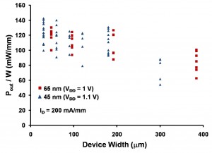
Figure 1: Normalized output power as a function of device width for 65 nm and 45 nm CMOS devices. The spread in data for each device width is due to measurements at multiple frequencies.
The remarkable improvement in the frequency response of silicon CMOS devices in recent years has motivated their use in millimeter-wave power applications, such as high-capacity wireless LANs, short-range high-data-rate wireless personal-area networks, and collision-avoidance radar for automobiles. A key concern in using CMOS for these applications is the inability of CMOS to yield high-efficiency power amplifiers with power levels over 10 mW in the 60-80 GHz regime. Our work investigates the fundamental limitations of Si CMOS in power amplification and explores options for device optimization with the goal of enhancing the millimeter-wave power-handling ability of Si CMOS.
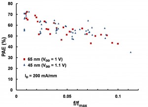
The key to obtaining high power is to increase the device width. However, increasing the device width results in a decrease in the normalized output power (Pout/W), thus limiting the maximum power obtainable from a given technology [1]. Figure 1 shows the decrease in normalized output power with device width for 65 nm and 45 nm CMOS devices from IBM. The main reason for this degradation is the non-ideal scaling of the ON resistance (Ron) with width in large devices. The peak power added efficiency (PAE) also shows a decrease with increasing device width [1]. In this case, the decrease is mainly due to the degradation in the maximum oscillation frequency (fmax) in wide devices. Figure 2 shows a strong correlation of PAE with fmax. As the frequency of operation approaches fmax, the gain decreases, resulting in degradation in PAE.
Figures 1 and 2 also show that IBM’s 65 nm and 45 nm technologies deliver similar output power and PAE. This is good news as circuit designers can take advantage of the higher integration density of 45 nm CMOS without losing any of the RF power performance of 65 nm technology.
To explain the fmax degradation in wide devices, small-signal equivalent circuits were extracted from the S-parameters measured on devices with different widths [2]. The results show that the intrinsic parameters (gm, Cgs and Cgd) are constant across width, but the extrinsic parasitic resistances (RD and RG) increase with increasing width. This work increases device width by wiring multiple unit cells in parallel. The additional wiring between the cells results in higher parasitic resistances, thus leading to a decrease in fmax and an increase in Ron for the wide devices. Hence, the key to enabling CMOS for millimeter-wave power applications is a parasitic-aware approach to designing wide devices.
References
- U. Gogineni, et. al, “RF Power Potential of 45 nm CMOS Technology,” Silicon Monolithic Integrated Circuits in RF Systems (SiRF), 2010, pp. 204-207. [↩] [↩]
- U. Gogineni, et. al, “Effect of Substrate Contact Shape and Placement on RF Characteristics of 45nm Low Power CMOS Devices,” Radio Frequency Integrated Circuits Symposium, 2009, pp. 163-166. [↩]
