Resonant-cavity-enhanced Mid-infrared Photodetector on a Silicon Platform
High-performance mid-infrared (mid-IR, i.e. 3-10 µm) photodetectors and imagers are attracting increasing interest recently due to their wide applications in security surveillance, chemical sensing, and industrial process monitoring [1]. Currently, most mid-IR detectors rely on single-crystalline semiconductors such as HgCdTe and III-V alloys for infrared absorption. While detectors and focal plane arrays (FPAs) based on these exotic alloys feature high quantum efficiency (QE), the FPAs have to be flip-chip bonded onto silicon readout-integrated circuits (Si ROIC) for signal readout and processing. Thermal expansion coefficient mismatch and poor mechanical stability often lead to low yields of such hybrid devices. Further, typical mid-IR detectors require a large absorber layer thickness (~10 µm) for high QE due to a low optical absorption coefficient in the mid-IR range.
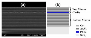
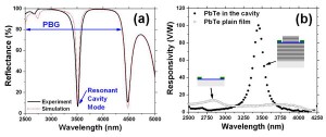
Here we demonstrate high-QE (90%) resonant-cavity-enhanced (RCE) mid-IR photodetectors fabricated monolithically on a silicon platform as shown in Figure 1. RCE design leads to near-unity QE at a much decreased absorber thickness and thus resolves the fabrication challenge associated with thick IR-absorber deposition. High-quality photoconductive polycrystalline PbTe film is thermally evaporated and acts as the IR absorber [2]. The entire detector structure can be directly deposited onto a silicon substrate free of lattice match constraints, enabling monolithic integration of mid-IR photodetectors with Si ROICs. The resonant cavity mode around 3.5 µm is identified by both optical and photoconductive measurements (Figure 2). In Figure 2(a), a comparison of the reflectance spectra of the cavity obtained by FTIR experiment and theoretical simulation shows excellent agreement. At resonant wavelength (3.5 µm), directly measured reflectance and transmittance values are 6.6 % and 3.5 %, respectively, indicating a QE of 90 %. In Figure 2(b), the RCE detector shows a peak responsivity of 100 V/W at 3.5 µm, 13.4 times higher than a blanket PbTe film of the same thickness.
- Figure 1: (a) SEM cross-sectional image of the resonant cavity structure deposited onto a SiO2/Si substrate. (b) Schematic picture of the designed structure. All fifteen layers are clearly seen in (a), demonstrating good film thickness control and uniformity. Sharp interfaces between different layers indicate no material inter-diffusion occurs since processing temperatures are low (< 160°C).
- Figure 2: (a) Reflectance spectra of the cavity structure obtained by FTIR measurement (solid line) and simulation (dotted line). The spectra show the resonant cavity mode at 3.5 µm as designed. (b) Responsivity spectra of the 100-nm PbTe thin-film photodetector within the cavity (filled circles) and without a cavity (plain film only, open circles). The two inserted pictures show the tested device structures schematically after metal deposition and patterning (green colored regions). Plain film shows much lower photoresponse (< 10 V/W) in the mid-IR range due to very weak light absorption, while PbTe in the cavity shows 13.4 times higher responsivity at the designed resonant wavelength.
References
- A. Rogalski, J. Antoszewski, and L. Faraone, “Third-generation infrared photodetector arrays,” J. Appl. Phys., vol. 105, 091101, 2009. [↩]
- J. Wang, J. Hu, X. Sun, A. M. Agarwal, L. C. Kimerling, D. R. Lim, and R. A. Synowicki, “Structural, electrical, and optical properties of thermally evaporated nanocrystalline PbTe films,” J. Appl. Phys., vol. 104, 053707, 2008. [↩]

