Re-architecting DRAM Memory Systems with Monolithically Integrated Silicon Photonics
The performance of future manycore processors will only scale with the number of integrated cores if there is a corresponding increase in memory bandwidth. Projected scaling of electrical DRAM architectures appears unlikely to suffice, being constrained by processor and DRAM pin-bandwidth density and by total DRAM chip power, including off-chip signaling, cross-chip interconnect, and bank access energy. In this work, we redesign the DRAM main-memory system using a proposed monolithically integrated silicon-photonic technology and show that our photonically interconnected DRAM (PIDRAM) provides a promising solution to all of these issues. Photonics provides high aggregate pin-bandwidth density through dense wavelength-division multiplexing (WDM). Photonic signaling provides energy-efficient communication, which we exploit not only to reduce chip-to-chip interconnect power but to also reduce cross-chip interconnect power by extending the photonic links deep into the actual PIDRAM chips. To complement these large improvements in interconnect bandwidth and power, we decrease the number of bits activated per bank to improve the energy efficiency of the PIDRAM banks themselves. Our most promising design point yields approximately a 10´ power reduction for a single-chip PIDRAM channel with similar throughput and area as a projected future electrical-only DRAM. Finally, we propose optical power guiding as a new technique that allows a single PIDRAM chip design to be used efficiently in several multi-chip configurations that provide either increased aggregate capacity or bandwidth.
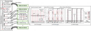
- Figure 1: Optical power-guided PIDRAM memory system. Each memory channel connects to a PIDRAM DIMM via a fiber ribbon. The memory controller manages the command bus (CB), write-data bus (WDB), and read-data bus (RDB), which all sit on the same fiber using WDM. Each PIDRAM chip can also have a number of different floorplans, shown on the right. Pn are photonics floorplans, where the number n represents the number of rows of data access points.
- Figure 2: Energy/bit breakdown of a single-chip PIDRAM channel for floorplans of three representative PIDRAM configurations: (a) 64 banks, 4 I/Os per array core; (b) 64 banks, 32 I/Os per array core; and (c) 8 banks, 32 I/Os per array core. E1 is the baseline electrical floorplan.

