PECVD CNT-enabled Electron-impact Gas Ionizers for Portable Mass Spectrometry

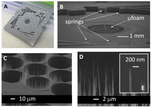
Figure 1: Field view optical picture of the ionizer’s main body (A), field view SEM of the central part of the main body showing the μfoam and the DRIE-patterned spring assembly system (B), field view SEM of a sparse PECVD CNT forest on top of the μfoam (C), close-up SEM of the PECVD CNTs (D), and close-up SEM of a CNT tip (E).
Research efforts on MEMS-based analytical instrumentation have focused on the development of rugged gas chromatography and mass spectrometry (GC/MS) systems that are smaller, lighter, cheaper, faster, and more power-efficient [1]. The power consumption, size, and weight of these systems are driven by the pump requirements. Therefore, relaxation of the pressure level at which the system components can operate would enable the systems’ portability. Portable GC/MS systems, either as individual units or as parts of massive networks, can be used in a wide range of applications including in-situ geological surveys, law enforcement, environmental monitoring, and space exploration [2].

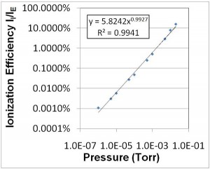
Figure 2: Ionization efficiency vs. pressure. Ideally, the data from electron-impact ionization describes a line with slope 1 using a log-log plot. The experimental data describes a line (R2=0.99) with slope 0.99.
The ionizer is one of the core components of an MS system. We have developed a carbon nanotube (CNT)-based MEMS/NEMS electron-impact gas ionizer with integrated extractor gate for portable mass spectrometry. The ionizer achieves low-voltage ionization using sparse forests of plasma-enhanced chemical-vapor-deposited (PECVD) CNTs as field-emitters and a proximal extractor grid with apertures aligned to the CNT forests to facilitate electron transmission. The extractor gate is integrated into the ionizer by using a high-voltage MEMS packaging technology based on Si springs defined by deep-reactive-ion etching (DRIE) [3]. The ionizer also includes a high aspect-ratio silicon structure (μfoam) that facilitates sparse CNT growth and also enables uniform current emission. The experimental data show that the MEMS extractor gate transmits up to 66% of the emitted current, and that the ionizers are able to produce up to 0.139 mA of ion current with up to 19% ionization efficiency at 22 mtorr while consuming 0.39 W [4]. Figure 1 shows a cross-section schematic and a picture of a fabricated ionizer; Figure 2 shows experimental data that demonstrate that the ionizers work as described by the electron-impact-ionization model.
References
- S. C. Terry et al, “A gas chromatographic air analyzer fabricated on a silicon wafer,” in Proceedings IEEE Trans. Electron Devices, vol. ED-26, no. 12, pp. 1880–1886, Dec. 1979. [↩]
- W. C. Wang, “Micromechanical devices at JPL for space exploration,” in Proceedings IEEE Aerosp. Conf., 1998, vol. 1, pp. 461–470. [↩]
- L. F. Velásquez-García, A. I. Akinwande, and M. Martinez-Sanchez, “Precision Hand Assembly of MEMS Subsystems Using DRIE-Patterned Deflection Spring Structures: An Example of an Out-of-Plane Substrate Assembly”, J. Microelectromech. Syst., vol. 16, no. 3, pp. 598–612, June 2007. [↩]
- L. F. Velásquez-García and A. I. Akinwande, “CNT-based MEMS/NEMS Gas Ionizers for Portable Mass Spectrometry Applications,” accepted for publication, J. Microelectromech. Syst., 2010. [↩]