Nanoscale Morphology at the Interface Between Colloidal Quantum Dots and Organic Semiconductor Films
The recent development of a hybrid organic/colloidal quantum dot light emitting device (QD-LED) consisting of a single monolayer of quantum dots (QDs) [1] highlights the need to establish rational control of nanoscale morphology, particularly at the interface of two dissimilar materials. The device structure consists of a close-packed monolayer of QDs sandwiched between two organic semiconductor charge-transport layers and carrier-injecting electrodes. The exact positioning of the QD monolayer affects the external quantum efficiency [2] [3]. We examine the degree of interpenetration at the interface between colloidal quantum dots and organic semiconductor molecules commonly employed in QD-LEDs, using tapping-mode atomic force microscopy. We compare different deposition methods, finding the greatest degree of QD penetration for a contact printed (Figure 1) QD layer. The QDs are spun cast onto a parylene coat polydimethylsiloxane (PDMS) “rubber stamp.” A substrate already coated with a thin film of organic material is brought into contact with this stamp and subsequently removed. The dots leave the stamp and are embedded in the organic film. We intentionally deposit a sub-monolayer of QDs in order to use tapping-mode atomic force microscopy to image the height at which the QDs emerge from the organic (Figure 2). The height variation of the background organic film is generally greater than the amount that the QD protrudes, requiring a mask to be defined to identify the locations of the QDs. The mask is defined by using the phase image (Figure 2b) from the atomic force microscopy scan, which shows a clear contrast between the QDs and the surrounding organic. After application of this mask to the height image, a histogram of the pixel heights is plotted (Figure 2c). The two roughly Gaussian distributions are easily identified, and the difference in the mean is recorded. The QDs protrude by about 0.7nm in Figure 2, which is a typical value across several different organic materials.
-
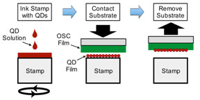
- Figure 1: Deposition method for quantum dots (QDs). A solution of QDs is spun-cast onto the stamp. A substrate with an organic film is brought into contact with the stamp and then removed. The QDs are transferred to the organic film.
-
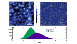
- Figure 2: Atomic force microscope data. (a) Topographic image of quantum dots (QDs) in an organic film. (b) Phase image. (c) Histograms of the pixel height of areas containing QDs (blue) and the background organic (green). The difference between the peaks indicates the height at which the dots emerge from the organic.

References
- P.O. Anikeeva, J.E. Halpert, M.G. Bawendi, and V. Bulović, “Quantum Dot Light-Emitting Devices with Electroluminescence Tunable over the Entire Visible Spectrum” Nano Letters, vol. 9, pp. 2532-2536, July 2009. [↩]
- P.O. Anikeeva, C.F. Madigan, J.E. Halpert, M.G. Bawendi, and V. Bulović, “Electronic and excitonic processes in light-emitting devices based on organic materials and colloidal quantum dots,” Physical Review B, vol. 78, pp. 085434 – 085438, 2008. [↩]
- P.O. Anikeeva, “Physical Properties and Design of Light-Emitting Devices Based on Organic Materials and Nanoparticles,” Ph.D. Thesis, Massachusetts Institute of Technology, Cambridge, MA, 2009. [↩]
Filed under: Nanotechnology |
Tags: katherine aidala, vladimir bulovic
![]() Print This Page
Print This Page
![]() Download as PDF
Download as PDF