Nanometrology

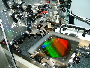
Figure 1: Photograph of the Nanoruler lithography and metrology system built by MIT students. This unique tool is the most precise grating patterning and metrology system in the world.
Manufacturing of future nanodevices and systems will require accurate means to pattern, assemble, image, and measure nanostructures. Unfortunately, the current state-of-the-art of dimensional metrology, based on the laser interferometer, is grossly inadequate for these tasks. While interferometers can be very precise when used in carefully-controlled conditions, they typically have an accuracy measured in microns rather than nanometers. Achieving high accuracy requires extraordinarily tight control of the environment and thus high cost. Manufacturing at the nanoscale will require a new technology for dimensional metrology that enables sub-1 nm precision and accuracy in realistic factory environments.

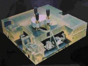
Figure 2: Photograph of reference block/sample holder for the Sub-Atomic Measuring Machine at the University of North Carolina – Charlotte.
A recently formed MIT-UNC–Charlotte team is developing a new metrology technology based on large-area grating patterns that have long-range spatial-phase coherence and ultra-high accuracy. Our goal is to reduce errors in gratings by 10-100 times over the best available today. These improved gratings can be used to replace interferometers with positional encoders to measure stage motion in a new nanomanufacturing tools and to calibrate the dimensional scales of existing nanofabrication tools. This increased precision and accuracy will enable the manufacturing of nanodevices and systems that are impossible to produce today. Improved dimensional accuracy at the nano-to-picometer scale will have a large impact on many nanotechnology disciplines including semiconductor manufacturing, integrated optics, precision machine tools, and space research.
As part of this effort, we will utilize a unique and powerful tool recently developed at MIT called the Nanoruler that can rapidly pattern large gratings with a precision well beyond other methods. Another unique high-precision tool, the UNCC-MIT-built Sub-Atomic Measuring Machine (SAMM), is being brought to bear to research new ways to quantify and reduce errors in the gratings.
Recent work at MIT is focused on improving the thermal controls in the Nanoruler lithography enclosure and developing an improved interferometer system to reduce errors in the stage metrology frame. At UNCC the SAMM is undergoing extensive refurbishment and improvements designed to boost interferometer accuracy.
References
- “Nanometer-level repeatable metrology using the Nanoruler,” P. Konkola, C. Chen, R.K. Heilmann, C. Joo, J. Montoya, C.-H. Chang and M.L. Schattenburg, J. Vac. Sci. Technol. B 21, 3097-3101 (2003).
- “Dimensional metrology for nanometer-scale science and engineering: towards sub-nanometer accurate encoders,” R.K. Heilmann, C.G. Chen, P.T. Konkola and M.L. Schattenburg, Nanotechnology 15, S504-S511 (2004).
- “Measuring two-axis stage mirror non-flatness using linear/angular interferometers,” J. Montoya, R.K. Heilmann and M.L. Schattenburg, Proc. of the 19th Annual Meeting of the American Society for Precision Engineering, Vol. 34, 382-385 (2004).
- “Optimization and temperature mapping of an ultra-high thermal stability environmental enclosure,” Y. Zhao, D.L. Trumper, R.K. Heilmann and M.L. Schattenburg, J. Precision Engineering 34, 164–170 (2010).