Nano-enabled Cold Cathodes for High-Frequency Vacuum Amplifiers
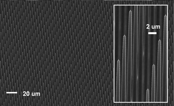
The continued demand for very wideband communications and the increased need for wireless channel capacity have led to the exploration of new regions of operation. In particular, the broad minimum in atmospheric absorption that occurs between 200GHz and 300 GHz is largely under-utilized because of a lack of high-bandwidth and high-power amplifiers in this frequency range that are compact and efficient. The core of the vacuum amplifier technology that we propose is a field-emitter-array (FEA) cathode that implements individual emitter ballasting to mitigate the effects of the emitter tip radii spread in the performance of the cathode. Specifically, emission currents are extremely sensitive to tip radii variation due to the exponential dependence of the emitted current on the tip radius of the emitter [1]. Unfortunately, tip radii distribution in FEAs has long tails [2]. By limiting the current from each emitter, it is possible to prevent destructive emission from the sharper tips while allowing higher overall current emission because of the emission of the duller tips. Ungated FETs are ideal to individually ballast each emitter because they behave like current sources and can be fabricated with high emitter density FEAs [3]. We have developed the technology for massive FEAs that are individually ballasted using vertical ungated FETs (Figure 1). We have demonstrated fully-controlled electron emission with currents as high as 0.6 A and with no damage to the cathode (Figure 2).
-
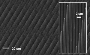
- Figure 1: A massive array (1-million units in 1 cm2) of individually ballasted field-emitters using very high-aspect-ratio vertical ungated FETs.
-
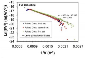
- Figure 2: Fowler-Nordheim (FN) plot of the data from an individually ballasted FEA cathode made of silicon with a resistivity equal to 178 Ω.cm. The data of an unballasted FEA describes a straight line in the Fn plot. The bending of the curve for high voltages is direct evidence of current control.

References
- R. Gomer, Field Emission and Field Ionization, American Institute of Physics, New York, 1961. [↩]
- M. Ding, G. Sha, and A. I. Akinwande, “Silicon Field Emission Arrays With Atomically Sharp Tips: Turn-On Voltage and the Effect of Tip Radius Distribution,” IEEE Transactions on Electron Devices, vol 49, No. 12, Dec. 2002, pp. 2333 – 2342. [↩]
- L. F. Velásquez-García, B. Adeoti, Y. Niu, and A. I. Akinwande, “Uniform High Current Field Emission of Electrons from Si and CNF FEAs Individually Controlled by Si Pillar Ungated FETs,” Technical Digest IEEE International Electron Device Meeting, Washington DC, USA, Dec. 2007, pp. 599 – 602. [↩]
Filed under: Nanotechnology |
Tags: akintunde akinwande, luis velásquez-garcía, stephen guerrera
![]() Print This Page
Print This Page
![]() Download as PDF
Download as PDF