Microscale Oscillating Crack Propagation in Silicon Nitride Thin Films

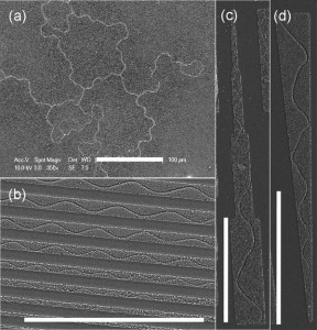
Figure 1: SEM images of a) random crack propagation in a continuous metal film and b-d) wavy crack propagation guided by patterned metal underlayers. Silicon nitride thin films were deposited to conformally coat metal films on silicon wafers coated with native oxides: on (a) a continuous metal film, (b) metal films patterned into lines, (c) lines with discrete width changes, and (d) lines with continuously varying widths. Samples were heated to 600C gas, the thickness of the metal patterns (Ag in this case) was 20 nm, and the thickness of silicon nitride films was 240 nm. All scale bars = 100µm.
Strain-induced cracking in thin films is a major concern during processing and can also lead to reliability issues. We are carrying out basic studies of cracks that develop in brittle films deposited on patterned metal layers, in order to better understand fracture mechanisms. Controlled microscale (<50 mm) wavy cracks in silicon nitride thin films have been observed in silicon nitride films deposited on metals with which they have poor adhesion.
Metal films, 20 nm thick, were deposited on oxidized silicon substrates using electron-beam evaporation. Lithographic patterning followed by a liftoff process was used to define metal patterns. The metal patterns consisted of 500-μm long lines, either with uniform widths with step changes in width, or with continuously varying widths. Samples with a variety of silicon nitride thicknesses (120, 150, 240 and 480 nm), and also with a variety of patterns of different metals (Au, Ag, Pt, Cu, Pd, Fe and Ti) were tested. Silicon nitride films were deposited over the exposed substrate to conformally coat the patterned metal using plasma-enhanced chemical-vapor deposition (PECVD), The samples were heated in forming gas (95 % nitrogen and 5 % hydrogen) to between 500 and 600°C, with a heating rate of 100°C/min to induce thermal stress. The samples were then allowed to cool at room temperature in the presence of the forming gas.

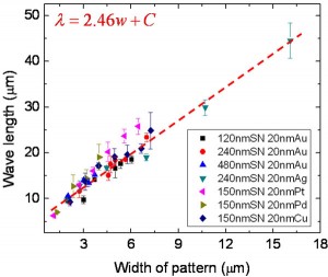
Figure 2: Relationship between the wavelength of a wavy crack and the width of the underlying metal pattern. “120nmSiN 20nmAu” indicates that the thickness of the silicon nitride thin film was 120 nm, and the thickness of the patterned Au pattern was 20 nm. The variable λ is the wave length of the wavy crack, w is the width of metal pattern, and C is a constant.
In many cases, cracks formed in the silicon nitride lying over the patterned metal films. For samples with Fe and Ti patterns, cracks, if they were observed, ran along the pattern boundary. Samples with Au and Ag led to random crack propagation (Figure 1a) or wavy crack propagation along the length of the patterned underlying film (Figure 1). The wavelengths and amplitudes of wavy cracks increased with an increase in the width of the metal patterns, with the amplitude of the wavy crack being half of the pattern width (Figure 2). This relationship was maintained when the patterns had step or gradual changes in their widths (Figures 1c and 1d). Wavy cracks could be initiated at specific locations at lower temperatures by pre-notching the patterns using a focused ion beam. Theoretical analyses of these results are underway.