Materials Reliability in GaN-based Devices
GaN-based devices, traditionally used for light-emitting diodes [1] [2], are becoming very attractive for high-power, high-frequency applications for a variety of radar and communication applications [3]. Of particular interest are AlGaN/GaN heterostructure-based high-electron-mobility transistors (HEMTs). Even though there has been extensive research done to improve these devices [4], their reliability is still a key issue and failure mechanisms are not well understood. The GaN films are typically in a state of high stress due to lattice and thermal mismatch. Moreover, the piezoelectric properties of GaN couple with high electric fields to add to the complexity of the mechanical stress state. The goals of this project are to identify the material failure mechanisms of GaN-based devices and to develop testing and lifetime projection methodologies.

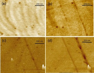
Figure 2: Progressive structural damage with voltage stress (a) unstressed device, (b) VDGstress=15 V< Vcrit, (c) VDGstress = 20 V≅ Vcrit,, (d) VDGstress=42 V, and (e) VDGstess = 57 V. (Arrows indicate the gate location.)
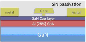
In the past year, we have investigated the surface morphology of electrically stressed AlGaN/GaN HEMTs (Figure 1) using atomic force microscopy and scanning electron microscopy after removing the gate metallization by chemical etching. We have correlated changes in the surface morphology with degradation in the electrical characteristics of the devices. We observe formation of linear grooves along the gate edges in the GaN cap layer for all electrically stressed devices. Beyond a critical voltage that corresponds to a sharp increase in the gate leakage current, we observe pit formation on the surface at the gate edges (Figure 2). The density and size of the pits increase with stress voltage and time and correlate with degradation in the drain current and current collapse. We believe that high mechanical stress in the AlGaN layer due to high-voltage electrical stressing is relieved by the formation of these defects, which act as paths for gate leakage current and result in electron trapping and degradation in the transport properties of the channel underneath.
Though thermally-enhanced, the diffusive processes that are required for groove formation and pit growth only occur in the presence of an electric field. As a consequence, both field and thermal enhancement must be accounted for, in reliability models for the associated degradation processes. Future work will investigate the diffusing species and mechanisms in order to develop reliability models for mass-transport-related failure.
References
- S. Nakamura and G. Fasol. The Blue Laser Diode. Springer-Verlag, Berlin, pg 343, 1997. [↩]
- T. Mikai, M. Yamada and S. Nakamura. Japanese Journal of Applied Physics, 38:3976, 1999. [↩]
- H. Okamura “Present Status and Future Prospect of Widegap Semiconductor High-Power Devices,” Japanese Journal of Applied Physics, 45, pp. 7565-7586, 2006. [↩]
- P. Saunier, C. Lee, A. Balistreri, D. Dumka, J. L. Jimenez, H.Q. Tserng, M. Y. Kao, P. C. Chao, K. Chu, A. Souzis, I. Eliashevich, S. Guo, J. del Alamo, J. Joh, and M. Shur, “Progress in GaN performances and reliability,” in Proc. IEEE DRC , pp. 35–36. Jun. 2007. [↩]
