Low-temperature Processed Lithographically Patterned Metal Oxide FETs for Integrated Circuits

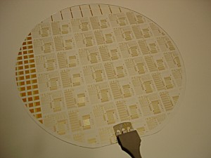
Figure 1: A 100-mm glass wafer with amorphous metal oxide field effect transistors fabricated in a low-temperature-budget (~100°C) process. The lithographic process enables integration of these FETs into large-area electronic circuits.
Metal-oxide-based field effect transistors (FETs) have been demonstrated with higher charge carrier mobilities, higher current densities, and faster response performance than amorphous silicon FETs, which are the dominant technology used in display backplanes [1] [2]. Although amorphous semiconductors are conventionally regarded as materials with low carrier mobilities and poor carrier transport, amorphous metal-oxide semiconductors are unaffected by the bond angle disorder that degrades performance in covalent semiconductors such as a-Si [3]. Because the optically transparent semiconducting oxide films can be deposited at near-room temperatures, these materials are compatible with future generations of large-area electronics technologies that require flexible substrates [4]. Our project aims to develop a low-temperature (~100°C), scalable lithographic process for amorphous metal oxide-based FETs that can be integrated into large-area electronic circuits.

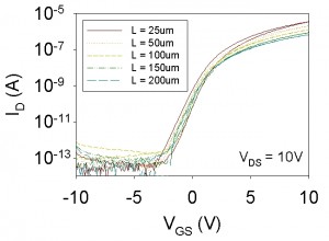
Figure 2: Transfer current-voltage characteristics for zinc indium oxide FETs with 10-nm-thick active layer and channel width = 100μm and varying channel lengths. Each transfer curve shown is double-swept. Gate leakage through the 280-nm-thick parylene dielectric is <1pA and on/off ratio > 107.
We have demonstrated top-gate, fully lithographic FETs on 100-mm glass wafers with a sputtered ZnO:In2O3 channel layer, using an organic polymer, parylene, as the gate dielectric and indium-tin-oxide (ITO) for source/drain contacts. The use of parylene, deposited by CVD onto room-temperature substrates in a solvent-free process, offers a pinhole-free, low leakage gate dielectric at much lower process temperatures compared to the inorganic dielectrics used in other reported fully lithographic processes [5]. Figure 1 shows a photograph of a 100-mm glass wafer after fabrication was completed; current-voltage characteristics for fabricated devices of varying channel lengths are shown in Figure 2. Current work focuses on using this baseline process as a platform for the design of oxide FET-based circuits, as well as for studying the underlying device physics of metal oxide FETs.
References
- R. L. Hoffman, B. J. Norris, and J. F. Wager, “ZnO-based transparent thin-film transistors,” Applied Physics Letters, vol. 82, pp. 733-735, Feb. 2003. [↩]
- T. Iwasaki, N. Itagaki, T. Den, H. Kumomi, K. Nomura, T. Kamiya, and H. Hosono, “Combinatorial approach to thin-film transistors using multicomponent semiconductor channels: An application to amorphous oxide semiconductors in In-Ga-Zn-O system,” Applied Physics Letters, vol. 90, art. no. 242114, June 2007. [↩]
- J. Robertson, “Disorder and instability processes in amorphous conducting oxides,” Physica Status Solidi B-Basic Solid State Physics, vol. 245, pp. 1026-1032, June 2008. [↩]
- E. Fortunato, P. Barquinha, G. Goncalves, L. Pereira, and R. Martins, “High mobility and low threshold voltage transparent thin film transistors based on amorphous indium zinc oxide semiconductors,” Solid-State Electronics, vol. 52, pp. 443-448, Mar. 2008. [↩]
- H. H. Hsieh and C. C. Wu, “Amorphous ZnO transparent thin-film transistors fabricated by fully lithographic and etching processes,” Applied Physics Letters, vol. 91, art. no. 013502, July 2007. [↩]