Logic Characteristics of 40-nm Thin-channel InAs HEMTs
As conventional Si CMOS scaling approaches the end of the roadmap, III-V based MOSFETs are being considered as an alternative technology to continue transistor size scaling [1]. In the quest to map the potential of III-Vs for future CMOS applications, the High-Electron-Mobility Transistor (HEMT) has emerged as a valuable model system to understand fundamental physical and technological issues. In fact, recently, excellent logic characteristics have been demonstrated in InAs HEMTs with gate length as small as 30 nm [2] [3]. This is mainly a result of the outstanding electron transport properties of InAs and the use of a thin quantum-well channel. Further scalability to Lg = 10 nm dimension characteristic of a future III-V CMOS technology will require harmonious scaling of all relevant device dimensions including the channel thickness. A consequence of a very thin channel is that carrier transport deteriorates, mainly as a result of increased carrier scattering. This can detract from performance.
In order to understand the trade-offs involved in thinning the channel in sub-100 nm III-V FETs, we have experimentally investigated the characteristics of InAs HEMTs with a 5-nm thick channel. This value is half that of earlier device demonstrations from our group [3]. We show that a very thin channel design substantially improves short channel effects (SCEs) and output conductance (go) characteristics but deteriorates its transport properties and access resistance. Future self-aligned gate (SAG) device architectures should be able to mitigate these problems.
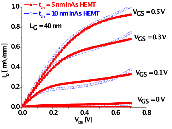
We have fabricated 40-nm gate length InAs HEMTs with a 5-nm thick channel [4]. The devices show excellent short-channel effects and scalability although their performance suffers from an increased source resistance. Figures 1 and 2 compare the output and subthreshold characteristics of InAs HEMTs with channel thickness of tch = 5 nm and tch = 10 nm. The device with tch = 5 nm exhibits S = 72 mV/dec, DIBL = 72 mV/V, and ION/IOFF = 2.5 x 10⁴, which are excellent values and represent substantial improvements over the thick channel device. The thin channel device also exhibits much better output conductance than the thick channel device. These encouraging results stem from the tight electron confinement afforded by the thin channel. However, this approach has trade-offs related to slightly degraded transport properties and access resistance. Neverthless, future self-aligned gate (SAG) device architectures should be able to mitigate these problems. This work suggests that future thin InAs channel MOSFETs have the potential for scaling to very small dimensions.
-
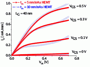
- Figure 1: Output characteristics for 40-nm gate length InAs HEMTs with channel thickness of 5 and 10 nm.
-
- Figure 2: Subthreshold and gate leakage characteristics for 40-nm gate length InAs HEMTs with channel thickness of 5 and 10 nm.
References
- D.-H. Kim et al, “Lateral and Vertical Scaling of In0.7Ga0.3As HEMTs for Post-Si-CMOS Logic Applications,” IEEE Tran. Electron Devices, Vol. 55, pp. 2546-2553, 2008. [↩]
- D.-H. Kim et al “Scalability of sub-100 nm thin-channel InAs PHEMTs,” Proceedings Indium Phosphide and Related Materials (IPRM), pp. 132-135, 2009. [↩]
- D.-H. Kim et al“30 nm E-mode InAs PHEMTs for THz and future logic applications,” Technical Digest on International Electron Device Meeting (IEDM), pp. 146-149, 2008. [↩]
- T.-W. Kim et al, “Logic Characteristics of 40 nm thin-channel InAs HEMTs,” Proceedings Indium Phosphide and Related Materials (IPRM), To be presented, 2010. [↩]
Filed under: Electronic Devices |
Tags: jesús del alamo, tae-woo kim
![]() Print This Page
Print This Page
![]() Download as PDF
Download as PDF