Integrated Graphene Interconnects with CMOS
As process technology scales, the importance of material and architectural innovation on interconnect performance will continue to increase. Graphene has attracted much interest as a replacement for copper interconnects due to its large conductivity and high current-carrying capacity [1] [2] [3]. Graphene sheets are also an attractive alternative to carbon nanotube-based interconnects as they are more compatible with conventional lithography methods. This project focuses on integrating high-density graphene devices and characterizing their properties as global interconnects.

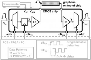
Figure 1: Diagram of experimental setup. The CMOS test chip includes an array of transmitters and receivers. Graphene is integrated directly on top of the CMOS chip and is electrically connected to each transmitter/receiver pair.
In this work, we characterize the performance of monolithically integrated graphene interconnects on a prototype CMOS chip (Figure 1). The test chip implements an array of transmitter/receivers to analyze the end-to-end data communication on graphene wires. Large-area graphene sheets are first grown by chemical vapor deposition [4] and transferred onto the CMOS chip. Subsequent lithography and etch steps were performed to complete the fabrication of graphene wires up to 1 mm in length. Each end of the graphene wire is electrically connected to the underlying transmitter/receiver pair. A low-swing signaling technique is applied, which results in a transmitter energy of 0.3-0.7 pJ/bit/mm, and a total energy of 2.4-5.2 pJ/bit/mm. The low-swing design shows up to 3.3x improvement in energy-delay product over the full-swing design. Bit error rates below 2×10⁻¹⁰ are measured using a 231-1 pseudo-random binary sequence at data rates between 10-25 Mbps. Minimum voltage swings of 100mV at 1.5V supply, and 500mV at 3.3V supply have also been demonstrated. The channel delay of a graphene wire is still an order of magnitude higher than that of a minimum-width CMOS Al wire. The performance of the graphene wire is largely limited by its growth quality and high sheet resistance.
References
- X. Du, I. Skachko, A. Barker, and E. Y. Andrei, ”Approaching ballistic transport in suspended graphene,” Nature Nanotech., vol. 3, no. 8, pp. 491–495, 2008. [↩]
- R. Murali, Y. Yang, K. Brenner, T. Beck, and J. D. Meindl, “Breakdown current density of graphene nanoribbons,” Appl. Phys. Lett., vol. 94, no. 24, p. 243114, 2009. [↩]
- A. Naeemi and J. Meindl, “Conductance modeling for graphene nanoribbon (gnr) interconnects,” IEEE Electron Device Lett., vol. 28, no. 5, pp. 428–431, May 2007. [↩]
- A. Reina, X. Jia, J. Ho, D. Nezich, H. Son, V. Bulovic, M. S. Dresselhaus, and J. Kong, “Large area, few-layer graphene films on arbitrary substrates by chemical vapor deposition,” Nano Lett., vol. 9, no. 1, pp. 30–35, 2009. [↩]