InGaAs MOS Transistor for Advanced Logic Application
For modern electronic devices, the improvement of performance resulting from scaling is to a large extent attributed to the increase of injection velocity of electrons (or holes) from the source to the channel [1]. In Si-based logic MOSFETs, as the channel length decreases, the performance gain from device scaling will eventually saturate, even with strained-Si engineering. However, introduction of new channel materials can provide further increase of injection velocity and thus increased device performance. InGaAs, due to its superior electron transport properties, is emerging as a promising candidate for future CMOS extension [2] [3] [4].

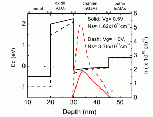
Figure 1: Design of InGaAs quantum well MOSFET with Al2O3 dielectric. The conduction band edge (left) and the carrier density (right) profiles are shown for Vg=0.5 and 1 V.
Previous work at MIT has studied the electron transport in InGaAs channel High-electron-mobility Transistors (HEMTs) and has experimentally shown promising injection velocity and intrinsic device delay [3] [4] . Yet, to apply the InGaAs channel transistor for VLSI application, it is imperative to add a gate dielectric in order to suppress the gate leakage current. The goal of this project is to fabricate and analyze a novel InGaAs quantum-well MOS transistor. A promising design of the InGaAs quantum-well MOSFET is illustrated in Figure 1. The conduction-band profile and carrier density in the cross section of the channel are computed by a 1-D Poisson-Schrödinger solver. The carrier concentration in the channel is effectively modulated by the gate voltage. At Vg=1 V this design provides an electron sheet carrier concentration of NS=1.62 x1012 cm-2 while at Vg=0 V, NS=2.03 x1010 cm-2 (not shown in the figure). The electron wave function is well-confined within the quantum well over the full range of transistor operation voltage.
One of the challenges in the fabrication of this MOS device lies in the growth of high-quality oxide on the III-V surface. We are in the process of optimizing the conditions of three steps on the MOS device: (i) the pre-gate surface preparation, (ii) atomic layer deposition (ALD) of dielectric, and (iii) post deposition annealing (PDA). Following this process optimization and integration, the scaling of InGaAs MOSFET and its performance comparison to the state-of-art silicon devices will be studied.
References
- D.A. Antoniadis, I. Aberg, C. Ni Chleirigh, O.M. Nayfeh, A. Khakifirooz, and J.L. Hoyt, “Continuous MOSFET performance increase with device scaling: the role of strain and channel material innovations” IBM Journal of Research and Development, vol. 50, pp. 363-376, July 2006. [↩]
- D.-H. Kim and J.A. del Alamo, “30 nm E-mode InAs PHEMTs for THz and Future Logic Applications,” in IEDM Tech. Dig., pp. 719-722, Dec. 2008. [↩]
- D.-H. Kim, J.A. del Alamo, D.A. Antoniadis, and B. Brar, “Extraction of Virtual-Source Injection Velocity in sub-100 nm III-V HFETs” in IEDM Tech. Dig., pp. 861-864, Dec. 2009. [↩] [↩]
- T.-W. Kim, D.-H. Kim, and J.A. del Alamo, “30 nm In0.7Ga0.3As Inverted-Type HEMTs with Reduced Gate Leakage Current for Logic Applications” in IEDM Tech. Dig., pp. 483-486, Dec. 2009. [↩] [↩]