In Situ Deposition of High-k Dielectrics on a III-V Compound Semiconductor in an MOCVD System

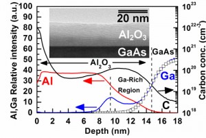
Figure 1: SIMS depth profile of elements C, Ga, and Al. The Ga and Al were plotted in relative intensity (left axis) while the C was plotted in atomic concentration (right axis). The open square symbols represent the fitted error function of the gallium profile. The inserted figure shows TEM image of the CVD oxide/GaAs structure.
We develop an in situ manufacturable method to passivate the III-V compound semiconductor (especially the GaAs) in an MOCVD system. The trimethyaluminum (TMA) and isopropanol (IPA) were chosen as the precursors of Atomic Layer Deposition (ALD) of Al2O3 ((C.W. Cheng and E.A. Fitzgerald,”In situ metal-organic chemical vapor deposition atomic-layer deposition of aluminum oxide on GaAs using trimethyaluminum and isopropanol precursors,” Applied Physics Letters, vol. 93, no. 3, pp. 031902:1-3, July 2008.)). The III-V channel and buffer layer were grown by the CVD mode, and then the passivation Al2O3 was deposited by ALD by applying appropriate procedures and growth parameters in the MOCVD system. This design made our CVD machine the first in situ passivation CVD machine in the world, and it achieved low interfacial defect density at an oxide/III-V semiconductor interface. Beside the in situ method, the ex situ method was investigated to compare the results with the in situ method; the self-cleaning effect was also explored in an ex situ process by applying TMA/IPA as ALD precursors [1]. Recently, in situ deposition of Al2O3 on GaAs was performed by Chemical Vapor Deposition (CVD) with the same precursors [2].

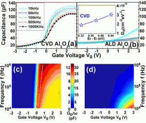
Figure 2: C-V characteristics of in situ (a) CVD and (b) ALD Al2O3 on GaAs. For the inserted figure in (b) Dit distribution of CVD samples in the band-gap extracted by the conductance-frequency method. (c) and (d) Gp/ω-Vg-f map of CVD and ALD samples. The dashed white line represents the position of the peak. The scales of maps (c) and (d) are different.
A gallium-rich region in the Al2O3 thin film above the interface was observed by using secondary-ion mass spectrometry (SIMS) depth profile measurement (see Figure 1). The X-ray photoelectron spectroscopy (XPS) results show that the gallium-rich region consists of Al2O3 and Ga2O3, but no As2O3 was observed. The gallium oxide was enriched above the interface during the deposition process. The layer of the Ga2O3– Al2O3 above the oxide/GaAs interface reduces the frequency dispersion of the Capacitance-Voltage (C-V) characteristics and lowers the interfacial defect density (see Figure 2). Both depletion and enhanced-mode MOSFET were fabricated to evaluate the real performance of the device with the in situ passivation oxide.
References
- C.W. Cheng, J. Hennessy, D. Antoniadis, and E.A. Fitzgerald, “Self-cleaning and surface recovery with arsine pretreatment in ex situ atomic-layer-deposition of Al2O3 on GaAs,” Applied Physics Letters, vol. 95, no. 8, pp. 082106:1-3, Aug. 2009. [↩]
- C.W. Cheng and E.A. Fitzgerald,”Improved interfacial state density in Al2O3/GaAs interfaces using metal-organic chemical vapor deposition,” Applied Physics Letters, (Accepted), May 2010. [↩]