Hybrid Organic/Quantum-dot Photodetector with Infrared Sensitivity
Hybrid structures consisting of colloidal quantum dots (QDs) and organic semiconducting materials have attracted a great deal of interest for photodetector device applications. Of particular interest is the prospect of infrared sensitivity with the incorporation of low bandgap QDs such as PbS and PbSe into hybrid organic/inorganic devices. This wavelength range is largely inaccessible to organic materials yet is critical to efficient photovoltaics as well as night vision and biological/chemical imaging applications.
Several hybrid organic/QD photodetector structures have recently been reported to exhibit good performance at infrared wavelengths. One study revealed an efficient charge-transfer mechanism from PbS QDs to the fullerene derivative, [6,6]-phenyl-C61-butyric acid methyl ester (PCBM) [1]. Another study described a hybrid device containing PbS QDs that was successfully integrated with amorphous silicon readout electronics to demonstrate the technical feasibility of making QD-based imagers [2].
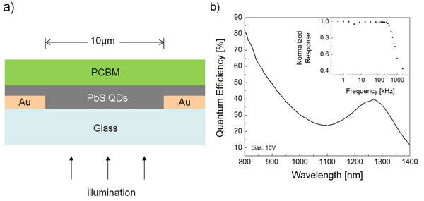
In this work we investigate charge and exciton dynamics at the PCBM/PbS QD hetero-interfaces through the experimental study of a photoconductor structure comprised of discrete layers of QDs and PCBM. A key feature of this lateral bi-layer device, distinguishing it from other reported hybrid devices, is that it unambiguously isolates the organic/QD hetero-interface as the site for interfacial charge and exciton recombination. Additionally, it affords great flexibility to modify the surface chemistry of the QDs without affecting the charge transport through the organic layer, thus making it a uniquely appropriate platform with which to study properties of the organic/QD hetero-interface.
Our findings elucidate the charge transport and recombination processes present in the PbS/PCBM system and suggest avenues for controlling these processes to optimize photodetector performance. Our optimized devices exhibit external quantum efficiencies above 20% at wavelengths extending to l=1.4mm (see Figure 1) and have frequency bandwidth of f3dB>100kHz (see Figure 1 inset).

Figure 1: (a) Schematic of PCBM/PbS QD bi-layer photodetector. (b) External quantum efficiency of a device with sensitivity extending to approximately 1400 nm. (inset) Frequency response of a typical device.
References
- K. Szendrei, F. Cordella, M. V. Kovalenko, M. Bӧberl, G. Hesser, M. Yarema, D. Jarzab, O. V. Mikhnenko, A. Gocalinska, M. Saba, F. Quochi, A. Mura, G. Bongiovanni, P. W. M. Blom, W. Heiss, and M. A. Loi, “Solution-Processable Near-IR Photodetectors Based on Electron Transfer from PbS Nanocrystals to Fullerene Derivatives,” Advanced Materials, 2009. [↩]
- T. Rauch, M. Bӧberl, S. F. Tedde, J. Furst, M. V. Kovalenko, G. Hesser, U. Lemmer, W. Heiss, and O. Hayden, “Near-infrared imaging with quantum-dot sensitized organic photodiodes,” Nature Materials, May 2009. [↩]