High-efficiency, Low-cost Photovoltaics using III-V on Silicon Tandem Cells
Photovoltaics and sustainability have received a lot of attention lately. We seek a tandem photovoltaic device using silicon as both the substrate and lower cell and GaAsP as the upper cell. The ideal band gaps for this two-cell tandem structure with silicon at 1.1eV and GaAsP at 1.75 eV allows access to the highest efficiency possible for a two-cell tandem, 36.5%. The lattice mismatch between GaP and Si is 0.37%; therefore, these two materials constitute a nearly ideal combination for the integration of Si and III–V semiconductor-based technologies. However, defect-free heteroepitaxy of GaP on Si has nevertheless been a major challenge.

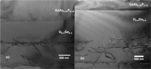
Figure 1: Cross-sectional <220> bright field TEM of GaAsyP1-y on (a) Si0.5Ge0.5 and (b) Si0.4Ge0.6 virtual substrates on 6° offcut towards the nearest {111} plane Si (001) substrate.
One can envision a process in which a Si1-xGex graded buffer is grown on a Si wafer to extend the lattice parameter part of the way to GaAs, at which point a lattice-matched GaAsyP1-y is grown on the Si1-xGex surface, followed by tensile grading of the GaAsyP1-y until GaP is reached. Identifying the composition where the transition can be made from Si1-xGex to GaAsyP1-y depending on the application is an integral objective of this study. This will provide the flexibility to engineer the lattice constants from Si to Ge and GaP to GaAs while maintaining low threadingdislocation density (TDD) and surface morphology suitable for device processing. In this study the successful growth of high-quality lattice-matched GaAsyP1-y on Si0.5Ge0.5, Si0.4Ge0.6, and Si0.3Ge0.7 virtual substrates has been achieved. Various characterization techniques clearly reveal a high-quality crystalline interface (Figure 1) between Si1-xGex and GaAsyP1-y with low TDD suitable for device processing, no rampant dislocation nucleation, anti-phase boundaries, or stacking faults and other crystalline defects. Further work will explore the temperature window for the epitaxial growth of GaAsyP1-y on Si1-xGex with higher Si content, as the end goal is to get a defect-free GaP film on Si substrate.