Graphene-based Ambipolar Electronics for RF Applications

Figure 1: Oscilloscope output demonstrating frequency doubling. The input frequency is 20 MHz and the output frequency is at 40 MHz. Graphene frequency doublers show excellent spectrum purity at the output without any filtering.
Since its discovery in 2004 [1], graphene has attracted great interest for novel electronic devices. Its extremely high electron and hole mobility [2], in combination with its high electron velocity and thermal conductivity, makes this material an excellent candidate for many high-frequency electronic applications. In addition, the unique ambipolar transport properties of graphene allow for completely new devices not possible in other materials, including non-linear electronics for RF and mixed-signal applications.

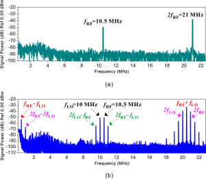
Figure 2: Spectrum analysis of a graphene mixer: (a) Output spectrum with single RF input fRF=10.5 MHz without LO signal. The frequency doubling is clearly visible. (b) Output spectrum with RF input fRF=10.5 MHz and local oscillator fLO=10 MHz at equal power. The presence of strong signal power at fRF – fLO=500 kHz and fRF + fLO=21.5 MHz demonstrates mixing operations.
In this work, we aim to demonstrate new device concepts for gigahertz applications based on the ambipolar transport properties of wafer-scale graphene grown by chemicals vapor deposition [3]. Several novel applications of graphene ambipolar devices have been demonstrated experimentally at a relatively low frequency. Figures 1 and 2 show graphene frequency doublers [4] and graphene ambipolar RF mixers demonstrated at 10s of MHz. Other applications of ambipolar electronics include ambipolar Binary Phase Shift Keying (BPSK) and folding amplifiers for analogue-to-digital converters. To enable these applications at GHz with excellent signal gain, graphene device dimensions need to be aggressively scaled. Recent results show that when the gate length is reduced from 5 μm to 1.5 μm, the current-gain cut-off frequency (fT) increases from less than 300 MHz to 1.5 GHz. In this project, we aim to shrink the gate length to sub-100-nm dimensions and also use T-shape gates to maintain a low gate resistance as gate length reduces. In parallel, we are developing the fabrication technology for these devices, especially the ohmic metallization and gate dielectrics, which are both critical to device performance. The former aims to find the optimal metal combination that will give stable contacts on graphene with low resistance and the latter aims to develop a reliable process for high-quality gate dielectric deposition for these field-effect transistors. We are also investigating various methods for depositing high-k materials and different polymer-based materials.
References
- K. S. Novoselov, A. K. Geim, S. V. Morozov, D. Jiang, Y. Zhang, S. V. Dubonos, I. V. Grigorieva, and A. A. Firsov, “Electric field effect in atomically thin carbon films,” Science, 306, pp. 666-669, 2004. [↩]
- K. I. Bolotin, et. al., “Ultrahigh electron mobility in suspended graphene” Solid State Communication,s 146, 351-355, 2008. [↩]
- A. Reina, et. al., “Large Area Few-Layer Graphene Films on Arbitrary Substrates by Chemical Vapor Deposition” Nano Letters, vol. 9, no. 1, pp. 30-35, 2009. [↩]
- H. Wang, D. Nezich, J. Kong, and T. Palacios, “Graphene Frequency Multipliers,” IEEE Electron Device Letters, vol. ED-30, no. 5, May 2009. [↩]