GaN Power Electronics
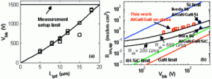
Our group is focusing on the development of GaN power transistors grown on Si substrates. Si substrates are preferred to SiC due to their much lower cost; however, GaN devices on Si substrates suffer from lower breakdown. To increase the breakdown voltage of AlGaN/GaN HEMTs grown on Si substrates, we have developed a new technology based on the removal of the original Si substrate and subsequent transfer of the AlGaN/GaN HEMT structure to an insulating carrier wafer (e.g., glass or polycrystalline AlN) [1]. By applying this new technology to standard AlGaN/GaN HEMTs with a total epitaxial thickness of only 2 mm grown on a Si substrate, AlGaN/GaN HEMTs transferred to a glass substrate with breakdown voltage above 1500 V and specific on-resistance of 5.3 mΩ·cm2 has been achieved, as shown in Figure 1.
The standard AlGaN/GaN HEMTs are depletion-mode (D-mode) devices. However, enhancement-mode (E-mode) devices are highly desirable for power electronics as they can greatly simplify circuit designs and improve system reliability. We have recently demonstrated a new AlGaN/GaN E-mode HEMT based on a dual-gate structure [2]. The device utilizes an integrated gate structure with a narrow gate controlling the threshold voltage and a long gate supporting the high voltage drop from the drain. Using this new dual-gate technology, AlGaN/GaN E-mode HEMTs grown on a Si substrate have demonstrated a high threshold voltage of 2.9 V with a maximum drain current of 434 mA/mm and a breakdown voltage of 643 V (Figure 2).
- Figure 1: (a) Three-terminal Vbk as a function of Lgd. (b) Specific Ron -Vbk plot of AlGaN/GaN HEMTs transferred to a glass wafer, compared with the highest breakdown voltages reported until now for an AlGaN/GaN-on-Si HEMT (total epitaxial thickness of 6 μm) and for an AlGaN/GaN-on-SiC transistor.
- Figure 2: (a) Id-Vds characteristics of a dual-gate E-mode device with Lgd = 5 μm; (b) Transfer characteristics of the dual-gate device and a D-mode device of the same structure without gate recess. The E-mode device is biased at Vds = 12 V and the D-mode device is biased at Vds = 10 V; (c) Three-terminal breakdown measurement at Vgs = 0 V. The resolution in the measurement of the gate leakage current is 1 μA/mm.
References

