Feature Scaling of Large, Ballasted Field Emission Arrays

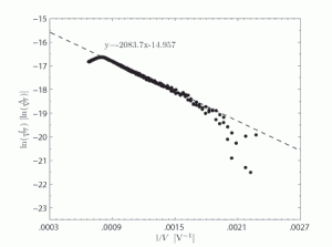
Figure 1: Fowler-Nordheim plot of a field-emitter ballasted by a 1 μm x 1 μm x 100 μm ungated FET pillar shows clear ballasting at large applied extraction gate voltages.
High current field emission arrays (FEAs) have garnered much interest in the areas of displays and microwave devices [1] [2]. While most of today’s research in field emitters has been performed with field emission display applications in mind, there is growing interest in using FEAs as the electron source in high-frequency vacuum electronics to amplify signals extending into the upper millimeter-wave spectral range, where conventional silicon electronics cannot efficiently operate.

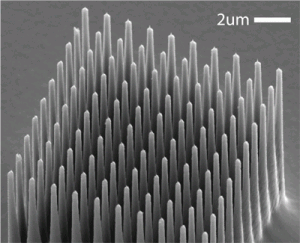
Figure 2: Scanning-electron micrograph of an array of field-emitters with their feature sizes scaled down. The pillars have a diameter of 250 nm and are 10 μm tall, with tip radius less than 10 nm.
Many FEA designs are hindered by non-uniform current emission. A central cause of this non-uniform emission is variation in the radius of each field emitter tip [3]. To combat this variability, we are ballasting each silicon field emitter tip by incorporating a high aspect ratio silicon pillar into each emitter [4]. The current in the pillar saturates at high drain-to-source voltages due to velocity saturation. This saturation results in current-voltage characteristics similar to that of an ungated FET. The current source-like behavior of the silicon pillar prevents destructive joule heating in the sharper tips while still allowing duller tips to emit, leading to higher overall current emission, better uniformity, and higher reliability.
To achieve higher packing density, the feature size of the ballasting ungated FET pillar is being scaled down. Current work has been building sharp emitters on pillars of dimensions 1 μm x 1 μm x 100 μm, which show clear ballasting (Figure 1). To scale the dimensions of the pillar down to 0.1 μm x 0.1 μm x 10 μm (Figure 2) while keeping the aspect ratio constant causes a reduction of the operating voltage. Simulations indicate that shrinking the dimensions of the FET to 0.1 μm x 0.1 μm x 10 μm results in a linear reduction of VDS,sat from 20V to 2V, indicating lower voltage operation.
References
- K.B.K. Teo, E. Minoux, L. Hudanski, F. Peauger, J. Schnell, L. Gangloff, P. Legagneux, D. Dieumegard, G.A.J. Amaratunga, and W.I. Milne, “Microwave devices: Carbon nanotubes as cold cathodes,” Nature, vol. 437, no. 7061, p. 968, Oct. 2005. [↩]
- J.D. Lee, I.H. Kim, C.W. Oh, J.W. Park, and B.G. Park, “MOSFET-controlled field emission display (MCFED),” in Vacuum Microelectronics conference, 2001. IVMC 2001. Proceedings of the 14th Internations, 2001, pp. 189-190. [↩]
- M. Ding, G. Sha, and A.I. Akinwande, “Silicon field emission arrays with atomically sharp tips: turn-on voltage and the effect of tip radius distribution,” IEEE Transactions on Electron Devices 49, no. 12, 2002. [↩]
- L.F. Velásquez-García, B. Adeoti, Y. Niu and A.I. Akinwande, “Uniform High Current Field Emission of Electrons from Si and CNF FEAs Individually Controlled by Si Pillar Ungated FETs,” Technical Digest IEEE International Electron Device Meeting, Washington DC, USA, Dec. 2007, pp. 599 – 602. [↩]