Fast Simulation of Pattern-dependencies in Thermal Nanoimprint Lithography

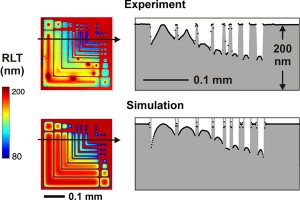
Figure 1: Comparison of an experimental imprinted topography with a feature-scale simulation, for a test-pattern imprinted into 200-nm-thick 495 kg/mol PMMA under a sample-average pressure of 40 MPa at 165 °C for 1 minute. The simulation tracks the differences between the residual layer thicknesses (RLT) of different features, as well as RLT variation within individual features. A simple Newtonian model of the resist and a linear-elastic model for stamp deflections capture much of the RLT variation observed.
A key challenge for putative industrial users of thermal nanoimprint lithography (NIL) is to design mask patterns that can be imprinted quickly enough and with rare enough defects to make the technique cost-effective. Specifically, heterogeneity of the shape, size, and areal density of imprinted features leads to elastic deflections of the imprinting stamp and/or to incomplete pattern replication. Critical-dimension variations can result: these variations need to be modeled and controlled through design. We are developing fast simulation techniques [1] [2] to help engineers assess the imprintability of chip-scale mask patterns and optimize layouts and processes.

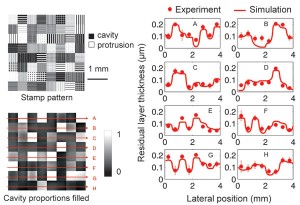
Figure 2: Experimental and simulated residual layer thicknesses for eight cross-sections through a feature-rich test pattern. The pattern was imprinted into 200 nm of 495 kg/mol PMMA resist under 16 MPa for 10 min at 180 °C. The simulation was performed using our pattern-abstraction method, and it illustrates the method’s ability to capture pattern-dependencies of RLT. The stamp cavities were 550 nm high, and also shown is a simulated map of the local proportions of cavity volumes filled by resist at the end of the imprinting cycle.
We encapsulate the resist’s mechanical behavior using an analytical function for its surface deformation when loaded at a single location. The stamp and substrate, meanwhile, are well modeled as linear-elastic; we distinguish between local stamp/substrate indentation and stamp bending, which we find to dominate when the spatial period of the pattern is more than about four times the stamp thickness.
Our approach takes a discretized stamp design and finds resist and stamp deflections in a series of steps. At each step, the algorithm iteratively finds the distribution of stamp–resist contact pressure that is consistent with the instantaneous compliances of the stamp and resist. Incremental changes in resist layer thicknesses are computed at each step by convolving the found pressure distribution with an appropriately scaled version of the resist’s point-load response. The system is then re-linearized for the next step.
We further accelerate the simulation of feature-rich patterns by pre-computing dimensionless relationships between pressure-history and pattern-replication for a variety of common feature shapes [3]. We can subdivide a given imprinting stamp into a grid of regions, each being assigned a characteristic feature shape, size, and areal density. Simulations of resist layer thickness represent experimental results in the literature to within ~10%. The insights provided by simulation allow us to propose NIL-specific layout design rules.
References
- H.K. Taylor and D.S. Boning, “Fast simulation of pattern dependencies in thermal nanoimprint lithography,” presented at Nanoimprint and Nanoprint Technology, San Jose, CA, Nov. 2009. [↩]
- H.K. Taylor and D.S. Boning, “Towards nanoimprint lithography-aware layout design checking,” Proc. SPIE, vol. 7641, 764129, 2010. [↩]
- H.K. Taylor, M.R. Hale, Y.C. Lam, and D.S. Boning, “A method for the accelerated simulation of micro-embossed topographies in thermoplastic polymers,” Journal of Micromechanics and Microengineering, vol. 20 no. 6, 065001, 2010. [↩]