Extraction Methodology on the Radius of Influence of STI and Polysilicon Pattern Density
Modern CMOS processes need new methodologies to extract, characterize, and model process variations and their sources [1]. Much work has been done to identify and characterize variation behaviors. The effort can be roughly divided into three groups as shown in Figure 1. The first group focuses on variation induced by changes in local layout geometries while keeping the pattern density constant across the chip [2] [3] [4]. The second group focuses on variation induced by changes in regional pattern density while keeping the transistor geometry constant [5]. This work falls into the third group: our goal is to consider variation when both local layout and regional pattern densities are changing and to study the interaction between regions of different pattern density. We propose a new methodology to extract the radius of influence, or the range of neighboring layout that should be taken into account in determining transistor characteristics, for shallow trench isolation (STI) and polysilicon pattern density. A new test chip, with 130k devices under test (DUTs) and step-like pattern-density layout changes, is designed in 65-nm technology as a case study. The extraction result of the measured data, shown in Figure 2, suggests that the radius of influence is limited to within the DUT cell size of 6 μm x 8 μm. For this technology, local layout geometry is the main contributor to systematic device variation. A simple post-layout extraction tool, which takes into account local layout features, is sufficient to capture the majority of the systematic component of the variability resulting from layout. Averaging across medium-range neighboring layout pattern densities to predict transistor characteristics is not necessary in the design flow for this technology.
-
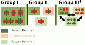
- Figure 1: Methods used in layout-dependent variation studies.

-
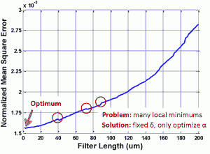
- Figure 2: Radius-of-influence (spatial averaging filter length) extraction based on measured data, showing that only local pattern density has an impact on transistor drain current in this technology.

References
- S. Borkar, “Designing reliable systems from unreliable components: the challenges of transistor variability and degradation,” IEEE Micro, vol. 25, pp. 10-16, Nov.-Dec. 2005. [↩]
- L.-T. Pang and B. Nikolic, “Measurements and Analysis of Process Variability in 90 nm CMOS,” IEEE Journal of Solid-State Circuits, vol. 44, no. 5, May 2009. [↩]
- H. Tsuno, K. Anzai, M. Matsumura, S. Minami, A. Honjo, H. Koike, Y. Hiura, A. Takeo, W. Fu, Y. Fukuzaki, M. Kanno, H. Ansai, and N. Nagashima, “Advanced Analysis and Modeling of MOSFET Characteristic Fluctuation Caused by Layout Variation,” pp. 204-205, IEEE Symposium on VLSI Technology, June 2007. [↩]
- K. Getting and D. Boning, “Study of CMOS Process Variation by Multiplexing Analog Characteristics,” IEEE Trans. On Semiconductor Manufacturing, vol. 21, no. 4, Nov. 2008. [↩]
- I. Ahsan, N. Zamdmer, O. Glushchenkov, R. Logan, E. Nowak, H. Kimura, J. Zimmerman, G. Berg, J. Herman, E. Maciejewski, A. Chan, A. Azuma, S. Deshpande, B. Dirahoui, G. Freeman, A. Gabor, M. Gribelyuk, S. Huang, M. Kumar, K. Miyamoto, D. Mocuta, A. Mahorowala, E. Leobandung, H. Utomo, and B. Walsh, “RTA-Driven Intra-Die Variations in Stage Delay, and Parametric Sensitivities for 65nm Technology,” pp. 170-171, Symposium on VLSI Technology, 2006. [↩]
Filed under: Electronic Devices |
Tags: albert chang, duane boning
![]() Print This Page
Print This Page
![]() Download as PDF
Download as PDF