Enhanced Hole Mobility in Narrow-channel Silicon/Germanium Core/Shell Nanowire Transistors

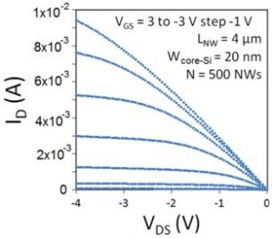
Figure 1: Output characteristics of a Si/Ge core-shell NW p-MOSFET with N= 500 parallel NWs and core-Si width of 20 nm.
Multi-gate semiconductor nanowires (NWs) have recently drawn significant attention as potential channel structures in high-performance metal-oxide-semiconductor field-effect-transistors (MOSFETs) due to their excellent gate control and immunity to short channel effects [1]. In addition, new channel materials such as Ge and SiGe are of great interest due to their higher mobility compared to Si. Thus, the incorporation of Ge in a multi-gate NW device architecture has the potential to fulfill the ultimate device requirements for electrostatics and current drive. In this work, Si-core/Ge-shell nanowire p-channel MOSFETs with high-K dielectric (Al2O3)/metal-gate (Tungsten Nitride (WN)) have been successfully demonstrated by selective epitaxial growth of Ge thin-films on the Si-nanowires fabricated by a top-down scheme [2].

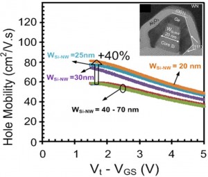
Figure 2: Effective hole mobility of Si-core/Ge-shell NW MOSFETs for various WSi-NW in the range of 20–70 nm calculated from low-field conductance and measured inversion charge capacitance. Inset shows XTEM of Ge/Si NW with Al2O3/WN gate stack.
Figure 1 shows the output characteristics of a Si/Ge core-shell NW MOSFET with 500 parallel NWs and with core-Si width of 20 nm. Cross-sectional transmission-electron-microscopy (XTEM), shown in the inset of Figure 2, reveals that the epitaxial Ge shell exhibits hexagonal (111) facets. Figure 2 shows the effective hole mobility of these long-channel NWs (L=4 µm), calculated using low-field conductance and split capacitance-voltage measurements after cancellation for parasitics. It is observed that the hole mobility increases by 40% as the Si-core size is decreased from 70 to 20 nm. Finite-element simulations of the stress profile induced in the Ge channel by the gate stack suggest that a transformation in the transverse stress component from compression to tension plays a role in the mobility enhancement. In addition, the mobility enhancement could be attributed to the increased population of the holes in (111) Ge sidewall facets, as compared to the top (100) planes which represent higher surface roughness.
References
- Suk et al., “High Performance 5nm radius Twin Silicon Nanowire MOSFET (TSNWFET): Fabrication on Bulk Si Wafer, Characteristics, and Reliability,” in IEEE IEDM Tech. Dig., 2005, pp. 717–720. [↩]
- P. Hashemi, M. Kim, J. Hennessy, L. Gomez, D. A. Antoniadis, and J. L. Hoyt, “Width-Dependent Hole Mobility in Top-Down Fabricated Si-Core/Ge-Shell Nanowire Metal-Oxide-Semiconductor-Field-Effect-Transistors,” Applied Physics Letters, vol. 96, p. 063109, 2010. [↩]