Electroquasistatic Sensors for Imaging IC Features
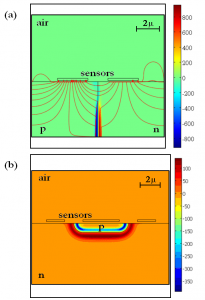
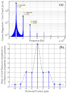
A technique for locating junctions in an integrated circuit with electroquasistatic sensors is under development for imaging purposes. An array of coplanar sensors is scanned laterally at a fixed height over the surface of a doped semiconducting bulk. Electric fields from the sensors can penetrate the surface of the semiconductor when the sensors are operated at a frequency comparable to the charge-relaxation frequency of the semiconductor. The challenge is to determine whether driven EQS electrodes can couple into p-n junctions without making any direct electrical contact with the semiconducting bulk. Figure 1a shows a finite element simulation where AC driven electrodes manage to forward-bias a p-n junction to a depth of approximately 2μm from a scan height of 0.1μm. If electrodes are positioned so that they are located away from any junctions, then the current on these sensors will be linear and experience no harmonic distortion. However, if two of these electrodes are located over the top of a p-n junction, then they couple into that junction, causing harmonic distortion in the sensors’ AC currents. Figure 2a shows an FFT of the center electrode’s current from the array in Figure 1b when the sensors are driven by a 1GHz voltage; a strong harmonic distortion is witnessed. Figure 2b illustrates how the harmonic distortion experienced by the center electrode from Figure 1b is maximized when the sensors straddle the p-well junctions and diminishes to zero when sensors are no longer located above the p-well. A large array of these electrodes could scan over the surface of a semiconductor with the individual sensor currents monitored for harmonic distortion. This concept could then provide a new, fast-scanning method for mapping and imaging the semiconducting layers of an integrated circuit, where wells and junctions are located by looking for harmonic distortion in the sensor-current frequency spectrum. Though not shown here, such a system can also distinguish conducting and dielectric features.
- Figure 1: Finite element simulation results of AC voltage-driven coplanar sensors held at a fixed scan height above doped silicon. Figure 1a shows electric field lines (red streamlines) and space-charge density [C/m3] (colormap) with sensor pair driven differentially with 15V peak-AC voltage at 5GHz. Sensors manage to couple into the junction to a depth of approximately 2μm from a scan height of 0.1μm. Figure 1b shows a space charge density [C/m3] colormap for a second simulated geometry with undriven sensors straddling the p-well’s depletion region.
- Figure 2: Evidence of harmonic distortion in the current on the center electrode from Figure 1b when driven by 1GHz voltage. Figure 2a provides an FFT of this sensor’s current whenthe sensor array is centered over the p-well. Figure 2b provides the ratio of the second harmonic amplitude to the first harmonic amplitude for the same sensor’s current vs. the array’s horizontal position relative to the p-well. Harmonic distortion is maximized when the sensors straddle the p-well junctions (as shown in Figure 1b) and drops to zero when sensors are no longer located above the p-well.

