Electron-impact-ionization Pump using Double-gated Isolated Vertically Aligned Carbon Nanotube Arrays

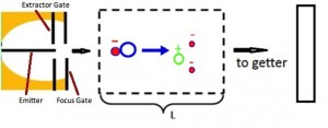
Figure 1: Electron-impact-ionization pump structure consists of a field-emission source (CNTs, an extractor gate and a focus gate), an electron-impact-ionization region (length of L) and an ion-implantation getter.
There is a need for microscale vacuum pumps that can be readily integrated with other MEMS and electronic components at the chip-scale level. Vacuum pumps exhibit favorable scaling and are promising for a variety of applications such as low-power portable mass spectrometers and sub-mm wavelength vacuum amplifiers. This project aims to develop the technology for a micro-fabricated electron-impact-ionizer pump. The micropump consists of a field-emission electron source that is an array of double-gated isolated vertically aligned carbon nanotubes (VA-CNTs), an electron-impact-ionization region, and an ion implantation getter, as shown in Figure 1. The pump works as follows: first, electrons are field-emitted from the VA-CNT array; then, the electrons are accelerated at a bias voltage that maximizes the probability of collision with neutral gas molecules, this way achieving ionization by fragmentation of the molecules; finally, ions are implanted into the getter.
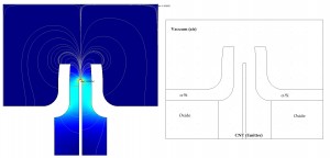
Figure 2: The solution of the electric field for an emitter of 20 nm tip radius, 1 µm height, and 0.24 µm gate aperture. A field factor (βG) of 2.1×10⁵ V/cm is obtained.
In a double-gated field-emitter array, the first gate (extractor) is used to extract electrons out of the tip, while the second gate (focus) is biased at a lower voltage than the first gate or emitter to focus the emitted electrons and collect the back-streaming ions, thus protecting the tip [1]. In this work, we are designing and simulating double-gated isolated VA-CNT field-emission arrays to study how the field-emitter tip position relative to the two gates affects the device performance. To quantify the effectiveness of the gates to affect the total emission current, the gate field factor (βG) and the focus field factor (βF) are examined using the commercial simulation software COMSOL. Figure 2 shows a solution of electric field for an emitter with 20 nm tip radius and 1 mm height with 0.24 mm aperture from a single gate. From this simulation, we obtain a gate field factor of 2.1×10⁵V/cm.
References
- L.-Y. Chen, L. F. Velasquez-Garcia, X. Wang, K. Cheung, K. Teo, and A. I. Akinwande, “Design, Fabrication and Characterization of Double-Gated Vertically Aligned Carbon Nanofiber Field Emitter Arrays.” in Vacuum Nanoelectronics Conference, 2007, pp 82-83. [↩]
