Efficient Light-trapping in Silicon Nanohole Solar Cells

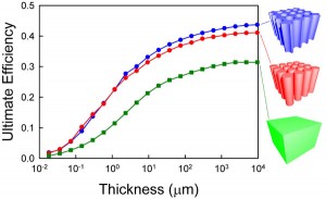
Figure 1: Calculated ultimate efficiency as a function of the thickness of the nanohole array, the nanorod array, and the homogeneous silicon film. The filling fraction and the lattice constant are 0.5 and 500 nm for the nanohole array, and 0.6 and 600 nm for the nanorod array, respectively. Note that nanohole arrays have an efficiency higher than nanorod arrays when the silicon thickness is greater than 2 µm.
The cost of crystalline silicon solar cells is expected to reduce significantly when the thickness of the silicon layer can be decreased from a few hundred to a few micrometers. However, the challenge in this case consists primarily of poor light absorption of crystalline silicon. Thus, an effective technique for light-trapping in thin active layers needs to be developed. In this work, we investigate silicon nanohole arrays as light-absorbing structures for solar photovoltaics via simulation.
Nanorod arrays are currently gaining considerable interest for solar photovoltaic structures because they can offer not only efficient carrier collection but also strong light-trapping [1] [2] [3]. An alternative structure would be their inverse structure, i.e., nanohole arrays [4]. Our calculations show that nanohole arrays have an efficiency superior to nanorod arrays for practical thicknesses as shown in Figure 1. To obtain the same ultimate efficiency as a standard 300-μm crystalline silicon wafer, we find that nanohole arrays require six times less thickness of silicon layers, which is equivalent to a twelve-times reduction in silicon mass. Our analyses reveal that the predicted high efficiency of nanohole arrays is due to both good optical coupling and strong light-matter interaction. With well-established fabrication techniques, nanohole arrays have great potential for efficient solar photovoltaics.
References
- B. Tian, X. Zheng, T.J. Kempa, Y. Fang, N. Yu, G. Yu, J. Huang, and C.M. Lieber, “Coaxial silicon nanowires as solar cells and nanoelectronic power sources,” Nature, vol. 449, pp. 885-889. Oct. 2007. [↩]
- B.M. Kayes, H.A. Atwater, and N.S. Lewis, “Comparison of the device physics principles of planar and radial p-n junction nanorod solar cells,” Journal of Applied Physics, vol. 97, pp. 114302:1-11, June 2005. [↩]
- M.D. Kelzenberg, S.W. Boettcher, J.A. Petykiewicz, D.B. Turner-Evans, M.C. Putnam, E.L. Warren, J.M. Spurgeon, R.M. Briggs, N.S. Lewis, and H.A. Atwater, “Enhanced absorption and carrier collection in Si wire arrays for photovoltaic applications,” Nature Materials, vol. 9, pp. 239-244, Feb. 2010. [↩]
- S.E. Han and G. Chen, “Optical absorption enhancement in silicon nanohole arrays for solar photovoltaics,” Nano Letters, vol. 10, pp. 1012-1015, Feb. 2010. [↩]