Digital Phase-tightening for Millimeter-wave Imaging
Millimeter-wave imaging has potential applications such as collision-avoidance radar at 77GHz and concealed-weapons detection at 77GHz, 94GHz, and higher. This research investigates the challenges of designing a millimeter-wave (MMW) imaging system. We envision an active imaging receiver that will consist of an array of 1000 antennae and per-antenna processor (PAP) units with an operating frequency of 77GHz. Each PAP has digital logic that will estimate the phase and amplitude and reduce the data rate to the order of a kilohertz. A central processing unit (CPU) will perform digital beamforming on the aggregated data from the array to achieve an expected frame rate of 10 fps. We aim to achieve 6-cm resolution at 30-m distance, or a beamwidth of 0.1º, which corresponds to time delays between antenna elements on the order of femtoseconds. Phase noise from the MMW front-end circuits will introduce jitter on the order of picoseconds, which will degrade the quality of the phase estimate.

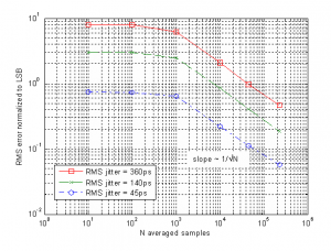
Figure 2: Measured RMS error versus number of averaged samples for different levels of timing jitter.
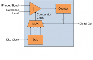
We introduce a technique called digital phase-tightening to estimate the phase in the presence of noise. This estimation is achieved by leveraging the large ratio between the MMW carrier frequency and the relatively low frame rates in imaging applications. By mixing down to an intermediate frequency and then averaging over many samples to estimate the phase, we reduce phase noise and attain phase error of the MMW beamformer in the femtosecond range. A test chip was designed and fabricated using the 0.13-µm CMOS devices in IBM’s BiCMOS8HP process. Figure 1 presents the block diagram of the circuits in the implemented system. These blocks operate after the received signal has been mixed down to the IF. The delay-locked loop (DLL) generates evenly delayed rising edges of the clock signal throughout its period. A simple comparator determines whether the IF input signal is above or below the zero reference level. A counter reads the comparator output and determines whether to incrementally increase or decrease the output of the DLL. The counter controls a MUX, which selects one of the delay taps from the DLL to clock the comparator near the zero-crossing of the input signal.
Figure 2 shows measured RMS error versus the number of averaged samples, N, for different levels of applied timing jitter. We observe that the RMS error level is directly related to the amount of jitter introduced, which we expect to see since more noise should result in larger error given the same amount of averaging. We also observe that the noise stays constant and then rolls off for increasing N. Once it rolls off, the error is reduced by 1/√N. The roll off is due to the bandwidth of the jitter. For the level of noise and averaging in the imaging system, we expect the RMS phase estimation error to be on the order of femtoseconds at the carrier frequency.
