Development of a Micromachined Retarding Potential Analyzer for Sensing Plasma Conditions at Spacecraft Re-entry
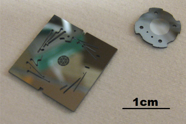
To ensure safe operation during space missions, NASA is sponsoring research on advanced sensing systems. In this endeavor, one particular facet is the development of a sensing skin that would monitor the spacecraft re-entry conditions. A retarding potential analyzer (RPA) is a device that would provide useful information about the ion energy distribution of the plasma that forms around the spacecraft while it re-enters the atmosphere. As a consequence of the harsh conditions during re-entry, the sensor must be made of suitable materials such as silicon carbide or tungsten. We are currently developing a hybrid MEMS-macro RPA that uses grids made of either bulk silicon coated with SiC or W. Design constraints of the RPA require closely packed holes with large aspects ratios. Therefore, the grids are etched using deep-reactive-ion-etching (DRIE). We plan to investigate the effects that various probe parameters have on the RPA’s performance, which is driven mainly by the Debye length of the plasma [1]. To this extent, the hybrid sensor has been designed to allow variations in grid hole diameter, pitch, and transparency. Limitations in grid-to-grid spacing will also be examined. The modular assembly of the device is shown in Figure 1. Based on this experimental exploration, a fully micromachined RPA will be built using a MEMS 3D packaging technology that we pioneered for multiplexed high voltage MEMS [2] [3]. An example of what this MEMS RPA may eventually look like is given in Figure 2, where the first grid is shown on the left and the collector plate is displayed on the right. The proposed MEMS RPA has five electrodes to insure proper data collection. Future work will further reduce the footprint of this final design as well as explore the possibility of machining the grids using bulk SiC.
-
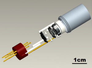
- Figure 1: Exploded view of a hybrid Retarding Potential Analyzer. The grids will be microfabricated in Si and coated with SiC or W; contact is made through pogo-pins and grids may be eliminated as deemed fit.

-

- Figure 2: Two-electrode Micro-RPA prior to hand-assembly. The first grid is the housing displayed on the left, and the collector to be assembled is shown on the right.
References
- I. H. Hutchinson, Principles of Plasma Diagnostics, 2nd ed., Cambridge: Cambridge University Press, 2002. [↩]
- L. F. Velásquez-García, A. I. Akinwande and M. Martínez-Sánchez, “Precision Hand Assembly of MEMS subsystems using DRIE-patterned deflection Spring Structures: An Example of an Out-of-plane Substrate Assembly”, Journal of Microelectromechanical Systems, Vol. 16, No. 3, pp. 598–612, 2007. [↩]
- B. Gassend, L. F. Velásquez-García, and A. I. Akinwande, “Precision In-Plane Hand Assembly of Bulk-Microfabricated Components for High-Voltage MEMS Arrays Applications,” Journal of Microelectromechanical Systems, vol. 18, no. 2, pp. 332-346, Apr. 2009. [↩]
Filed under: MEMS & BioMEMS |
Tags: akintunde akinwande, eric heubel, luis velásquez-garcía
![]() Print This Page
Print This Page
![]() Download as PDF
Download as PDF