Defect Formation around the Critical Voltage in Electrically Stressed GaN HEMTs

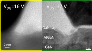
Figure 1: Cross-sectional TEM images of devices stressed at different voltages: right around Vcrit (left), and beyond Vcrit (right).
GaN-based electronics have been of great interest because of the high-breakdown electric field (>3×10⁶ V/cm) in this material system. Also, due to the strong piezoelectricity and spontaneous polarization of nitride semiconductors, a high sheet-carrier density (~1013 cm-2) can be easily obtained in the AlGaN/GaN heterostructure without any doping. In addition, high electron mobility (~1500 cm2/V-s) and high saturation velocity (~2×107 cm/s) make GaN high-electron-mobility transistors (HEMT), uniquely suitable for high power and high frequency RF power applications, such as WiMAX or WLAN base stations and radars.
In spite of promising performance results, GaN HEMTs still exhibit limited reliability. In RF power applications, GaN HEMTs must operate at a high voltage where good reliability is challenging. Physical understanding of the fundamental degradation mechanisms is essential to tackle reliability problems. In our previous studies, we have found that in GaN HEMTs, electrical degradation is electric-field-driven and is characterized by a sharp onset at a critical voltage Vcrit, beyond which various device performance parameters start to degrade [1]. This behavior has been explained through a model that invokes the creation of defects due to increased mechanical stress in the AlGaN barrier layer, introduced through the inverse piezoelectric effect at high voltage [1].
Cross-sectional transmission electron microscopy (TEM) has been one of the most efficient methods to study structural damage produced by electrical stress in GaN HEMTs after long-term life tests [2]. Crystallographic defects such as pits and cracks have been observed at the drain side of the gate corner in the GaN cap and AlGaN barrier layer. A correlation between the amount of electrical degradation and the degree of physical damage has also been reported [2]. However, no systematic study correlating stress voltage and crystallographic damage has been performed. To fill this gap is the goal of this work.
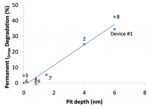
We have step-stressed identical GaN HEMT devices up to different voltages around and beyond Vcrit. These experiments were done on precisely matched devices and produced different level of electrical degradation. Through TEM analysis, we have found that this electrical degradation correlates well with the amount of structural damage at the semiconductor surface on the drain side right next to the gate corner. As shown in Figure 1, at around Vcrit (~15-17 V for this transistor technology under these conditions), a shallow pit in the GaN cap starts to be produced. At higher stress voltage, this pit grows, penetrating into the AlGaN barrier layer. By comparing the depth of these pits with the degradation in IDmax (Figure 2), we have confirmed that the observed crystallographic damage is responsible for the electrical degradation in these GaN HEMTs.
References
- J. A. del Alamo and J. Joh, “GaN HEMT reliability,” Microelectronics Reliability, vol. 49, pp. 1200-1206, 2009 [↩] [↩]
- U. Chowdhury, J. L. Jimenez, C. Lee, E. Beam, P. Saunier, T. Balistreri, S.-Y. Park, T. Lee, J. Wang, M. J. Kim, J. Joh, and J. A. del Alamo, “TEM observation of crack- and pit-shaped defects in electrically degraded GaN HEMTs,” IEEE Electron Dev. Lett., vol. 29, pp. 1098-1100, 2008 [↩] [↩]
