Co-axial Integration of III-V Ridge-waveguide Gain Elements with SiOxNy Waveguides on Silicon

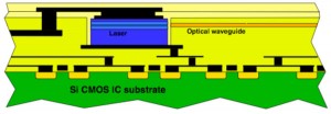
Figure 1: A cartoon illustrating the recess-mounting and co-axial alignment approach to integrating III-V gain elements (edge-emitting in-plane laser diodes, EELs, and semiconductor optical amplifiers, SOAs) with silicon oxy-nitride waveguides on silicon integrated-circuit chips and silicon photonic integrated-circuits platforms.
Our ongoing research integrating 1.55-µm III-V ridge waveguide gain elements (i.e., diode lasers and semiconductor optical amplifiers) co-axially aligned with and coupled to silicon oxy-nitride waveguides on silicon substrates has made significant strides in the past year. We are working towards the goal of co-axially coupling III-V laser diodes and semiconductor optical amplifiers with waveguides on Si wafers; to do so, we use techniques consistent with fabricating waveguides on Si-CMOS wafers and integrating the III-V gain elements after all standard front- and back-end Si processing has been completed.
A novel micro-cleaving technique has been used to produce active ridge waveguide platelets on the order of 6 µm thick and 100 µm wide, with precisely controlled lengths (in the current work 300 ± 1.25 µm) and very high-quality end facets. Typical ridge guide platelet lasers have thresholds under 30 mA.

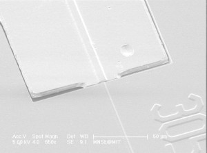
Figure 2: A close-up photomicrograph showing the alignment between an InGaAsP/InP ridge waveguide platelet and a buried silicon oxy-nitride waveguide. Coupling losses as low as 3 dB were measured.
Passive micro-cleaved platelets have been integrated within dielectric recesses etched through the oxy-nitride (SiOxNy) waveguides on a wafer so that the ridge and SiOxNy waveguides are co-axially aligned. Transmission measurements indicate coupling losses are as low as 5 db with air filling the gaps between the waveguide ends, and measurements made through filled gaps indicate that the coupling losses can be reduced to below 1.5 dB with a high index (n = 2.2) dielectric fill. Simulations indicate that with further optimization of the mode profile in the III-V waveguide, the loss can be reduced to below 1 dB.
We have also performed extensive device design and optimization for co-axial recess integration and have recently completed a comparison of co-axial coupling with the evanescently coupled III-V/Si hybrid integration approach recently introduced by researchers at UCSB and Intel. The latter comparison revealed that the approach we have taken, co-axial end-fire coupling, and the UCSB/Intel approach, vertical evanescent coupling, are complementary, with each optimal for certain applications. At the same time it pointed out a number of distinct advantages for co-axial coupling of recess-integrated platelet lasers including higher operating efficiency, smaller device footprint, greater flexibility in choice of materials, lower cost, higher modularity, and easier integration of different wavelength emitters [1].
References
- C.G. Fonstad, J.J. Rumpler, E.R. Barkley, J.M. Perkins, and S. Famenini, “Recess Integration of Micro-cleaved Laser Diode Platelets with Dielectric Wave-guides on Silicon,” Proc. of the Novel In-plane Semiconductor Lasers Conference VII, Photonics West 2008. 8, SPIE Conference Proc. vol. 6909, 2008, pp. 69090O-1 to 69090O-8, [↩]