CMOS-compatible Molecular Floating-gate Memories

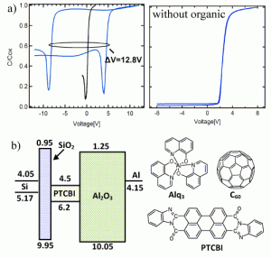
Figure 1: a) The C-V characteristic of devices with PTCBI/C60 and without organic layer, and b) energy-band diagram and chemical structure of organic materials.
Flash memory devices are now entering the sub-50-nm lithography regime. Flash cell scaling is always challenging because of the high electric fields required for the program and erase operations and the stringent leakage requirements for long-term charge storage. The electric-field requirements impose restrictions on the physical scaling of the memory; the diminishing number of stored electrons imposes restrictions on reliability. Overcoming these limitations will require innovations in cell structures and device materials, including proposals for replacing the polysilicon floating gate by segmented charge storage elements. With discrete charge storage, the impact of a defect is limited only to charge stored in its proximity and not to leaking of the conducting floating gate.

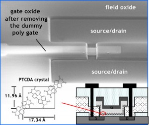
Figure 2: SEM image of memory transistor after removing the dummy poly gate and schematic cross section of the transistor.
This study investigates charge-storage behavior in a series of molecular thin films embedded in metal-oxide-semiconductor (MOS) structures with SiO2 and Al2O3 as the tunneling and control oxides, respectively. By comparing performance of different devices, we identify the molecular thin-film characteristics best suited for design of floating-gate memories. We fabricate capacitive memory structures using archetypical molecular thin films with different charge-storage energy levels and charge mobility including 3,4,9,10-perylenetetracarboxylic dianhydride (PTCDA), 3,4,9,10- perylenetetracarboxylic bis-benzimidazole (PTCBI), tris-(8-hydroxyquinoline) aluminum (Alq3), and fullerene (C60).
The stored charge densities are determined by measuring the shift in the flat band voltage of molecular-film-containing capacitors. Data shows that charge retention times are improved for molecular films with lower carrier mobility, which for the first time confirms the stated operational benefit of the nano-segmented floating-gate structures, i.e., that lower charge mobility in the nano-segmented floating gate inhibits stored charge loss.
The initial results show device durability over 105 program/erase cycles, with a hysteresis window of up to 12.8V, corresponding to charge storage density as high as 1.3 x 1013 cm-2.
As the next step we are working on fabrication of CMOS-compatible organic memory transistors using gate-last fabrication process, in which source and drain regions are defined using a dummy poly gate that is removed during the process.
References
- S. K. Lai, “Flash memories: successes and challenges,” IBM J. Res. & Dev., vol. 52, no. 4-5, pp. 529-535, 2008.
- P. Pavan, R. Bez, P. Olivo, E. Zanoni, “Flash Memory Cells-An Overview,” Proc. of the IEEE., vol. 85, no. 8, pp. 1248-1271, 1997.
- International Technology Roadmap for Semiconductors, ITRS, 2007. Available: http://www.itrs.net
- K. Kinam, “Technology for sub-50nm DRAM and NAND Flash Manufactureing,” IEDM, 1609340, pp. 323-326, 2005.