Anodic Aluminum Oxide Scaffolds for Nanowire Growth for Energy-storage Applications
Metallic nanowires are of interest for a number of energy-related applications such as micro-batteries, supercapacitors, and photocatalytic chemical conversion. To integrate synthesized nanowires into devices, it is desirable to fabricate them with controlled size, spacing, location, and ordering on the device -applicable substrates. As a strategy for this, we are developing templated self-assembly methods that combine top-down (lithography) and bottom-up (self-assembly) approaches for fabricating and assembling various metallic nanowires for energy storage applications [1].
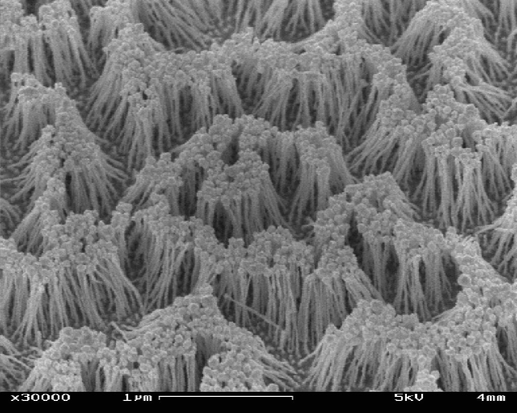
Ordered porous alumina (OPA) is a nano-structured material that self-orders with domains and has been widely used as a template for growth of metallic nanowires and nanotubes. However, the nanowires grown in the OPA are electrically blocked from the substrate due to a thin insulating barrier oxide at the base of the pores. While it is desirable to remove the thin barrier oxide, removal is normally done using chemical etching, a barrier-thinning technique, or a reverse-bias technique. These methods lead to pore-widening and are difficult to implement for OPAs on substrates. In earlier work we developed a new method for perforation of the OPA barrier layer, based on anodization of Al/W multilayer films on substrates [2], without changing the pore diameter. The combination of templating and use of this new pore-perforation technique allows fabrication of ordered pore arrays with pore spacings and diameters that can be independently varied (Figure 1). When Al/W multilayer films are anodized and pores approach the Al/W interface, tungsten oxide forms and penetrates the alumina barrier oxide. If we selectively etch the tungsten oxide, the barrier oxide can be removed and the base of the pores opened, without etching of the OPA (Figure 2). With this technique, we have demonstrated that it is possible to perforate OPA barrier layers for porous structures with small-diameter pores at small spacings and fabricated free-standing metallic nanowires, such as Ni, Au, and Pt, and carbon nanotubes on metallic layers on Si substrates (Figure 2) by selectively removing the OPA template. Using these NWs and NTs with or without the AAO as a platform, we are testing electronic characteristics for future IC interconnects and developing a micro-battery.
-
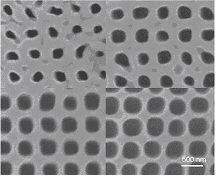
- Figure 1: Top-view of ordered porous alumina with fixed periods and varied diameters. Note that templating has imposed square symmetry over the natural hexagonal ordering.
-
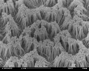
- Figure 2: Ordered arrays of high-aspect-ratio electrically-connected nanowire electrodes made by electrodeposition of Pt into porous alumina with ordered pore arrays. The alumina has been selectively removed after electrodeposition of the wires’ alumina. Note that the wire tips have clustered due to capillary forces during drying. If desired, this clustering can be avoided by using critical-point drying.
References
- R. Krishnan and C. V. Thompson, “Monodomain high-aspect-ratio 2D and 3D ordered porous alumina structures with independently controlled pore spacing and diameter,” Advanced Materials, vol. 19, pp. 988-+, Apr 6 2007. [↩]
- J. Oh and C. V. Thompson, “Selective barrier perforation in porous alumina anodized on substrates,” Advanced Materials, vol. 20, 1368, (2008). [↩]
Filed under: Energy |
Tags: carl thompson, yong cheol sun
![]() Print This Page
Print This Page
![]() Download as PDF
Download as PDF