Advanced Substrate Engineering: Integration of InP Lattice Constant on Si
Integration of the InP lattice constant with Si CMOS platforms is motivated by the monolithic interconnection of III/V optoelectronic and electronic devices with the highly integrated Si logic. However, integration of InP on Si requires a comprehensive solution that addresses lattice mismatch, thermal expansion mismatch, IV/III-V integration, and alloy engineering challenges.
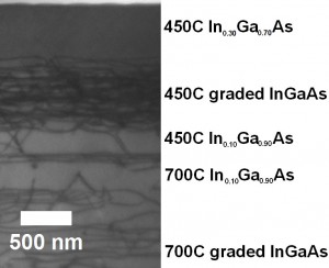
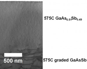
We investigated III/V graded (Ñ) buffers on 6˚ offcut GaAs substrate in combination with 6˚ offcut Ge-on-Insulator (GeOI) substrate to integrate the InP lattice constant on Si. First, we chose 6˚ offcut GeOI as the substrate to accommodate the antiphase disorder in the IV/III-V integration [1] and established excellent GaAs epitaxy on the substrate with proper surface preparation. Then we investigated two approaches to integrate III/V alloys up to InP lattice constant on 6˚ offcut GaAs: GaAs/ÑInxGa1-xAs/ÑInyGa1-yP/InP and GaAs/ÑGaAs1-xSbx. For the GaAs/ÑInxGa1-xAs/ÑInyGa1-yP/InP approach, we demonstrated the integration of InP on 6˚ offcut GaAs with threading dislocation density of 7.9×10⁶ /cm2 and surface roughness of 30.0 nm. The second approach used ÑGaAs1-xSbx alloys with compositional grading of the Sb concentration. Graded mixed-anion GaAsSb alloys grown at 575°C did not exhibit phase separation, resulting in higher quality InP lattice constant films on GaAs than the first method. A GaAsSb alloy (with a grading rate ~ 1.06% strain/um) lattice-matched to InP on 6° offcut bulk GaAs with threading dislocation density of 4.7×106 cm-2 and roughness of 7.4 nm was demonstrated. The threading dislocation density of the GaAsSb graded buffer can be further lowered to 2.7×106 cm-2 if a lower grading rate (0.64% strain/um) is used.
-
Figure 1: An XTEM of 6° offcut
GaAs/∇InxGa1-xAs/∇InyGa1-yP/InP.
-
Figure 2: An XTEM of 6˚ offcut
GaAs/∇GaAs1-xSbx/InP.
References
- S. M. Ting and E. A. Fitzgerald, “Metal-organic chemical vapor deposition of single domain GaAs on Ge/GexSi1-x/Si and Ge substrates,” Journal of Applied Physics, vol. 87, pp. 2618-2628, Mar. 2000. [↩]

