Active Photonics in a CMOS Platform
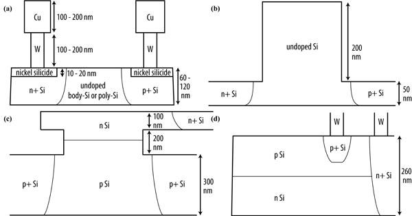
Although the majority of silicon photonic research is motivated by end applications where photonic devices can be integrated alongside millions of transistors, most research devices are fabricated in independent photonics-only process flows. Free from the constraints of working within an existing process, fabrication steps and layer geometries have been tailored to optimize the performance of individual devices. The short-flow methodology has enabled pioneering device research and proof-of-concept demonstrations by many academic and industrial groups [1]. The rapid progress in this work helped to lay the groundwork for the demonstration of a complete electronic-photonic integrated circuit (EPIC) platform by modifying a 130-nm SOI-CMOS platform to accommodate the required fabrication steps [2]. Today, however, prominent EPIC applications from multiprocessor interconnect [3] to coherent-communication receivers [4] require photonic devices to be integrated alongside the dense, high-performance transistors available only within state-of-the-art electronic processes. Recently, localized substrate-removal technology has enabled photonic device integration through the addition of a single post-fabrication step on designs fabricated in unmodified state-of-the-art CMOS electronic foundries [5]. By sharing all in-foundry processes, EPICs including state-of-the-art transistors can leverage the existing infrastructure and economy of scale provided by the orders-of-magnitude-larger electronics industry. The major constraint is to adapt the photonic device designs to be manufacturable within the existing process. This challenge is illustrated by comparing the scaled CMOS lateral p-i-n diode shown in Figure 1a to existing p-i-n diodes used as modulators within traditional silicon photonics processes shown in Figure 1b-d. Although the diode formed is electrically suitable for use as a carrier-injection modulator, the slab geometry does not allow for lateral optical confinement away from the optically-lossy electrical contacts. Therefore, novel diode design, perhaps including non-uniform patterning in the direction of propagation, is required to reduce integrate contacts with low optical loss.

Figure 1: (a) Slab waveguide CMOS modulator cross-section differs greatly from the geometries of previously demonstrated silicon modulators: (b) injection-mode rib waveguide p-i-n diode [1], (c) depletion-mode vertical junction rib waveguide [6], and (d) depletion-mode vertical junction slab waveguide diode [7].
References
- Q. Xu et al., “Micrometre-scale silicon electro-optic modulator,” in Nature 435, 325-327, (2005). [↩] [↩]
- C. Gunn, “Fully integrated VLSI CMOS and photonics ‘CMOS photonics’,” in VLSI Technology, 2007 IEEE Symposium on, 6-9 (2007). [↩]
- C. Batten et al., “Building many-core processor-to-DRAM networks with monolithic CMOS silicon photonics,” IEEE Micro 29, 8-21 (2009). [↩]
- C.R. Doerr et al., “Monolithic polarization and phase diversity coherent receiver in silicon,” J. Lightwave Technol. 28, 520-525 (2010). [↩]
- C.W. Holzwarth et al., “Localized substrate removal technique enabling strong-confinement microphotonics in a bulk CMOS process,” in Proc. CLEO/IQEC Conf. Lasers Electro Opt/Intl. Quant. Elec. Conf., Mar. 2008. [↩]
- A. Liu et al., “High-speed optical modulation based on carrier depletion in a silicon waveguide,” Opt. Express 15, 660-668, (2007). [↩]
- M.R. Watts, D.C. Trotter, and R.W. Young, “Maximally confined high-speed second-order silicon microdisk switches,” in Proc. Optical Fiber Communication Conf., Feb. 2008. [↩]