Accurate Mobility Measurements of Gate-all-around Si Nanowire p-MOSFETs with Conformal High-K/Metal Gate Stack

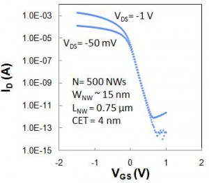
Figure 1: Measured transfer characteristics of ~15nm diameter gate-all-around nanowire p-MOSFETs with N=500 parallel nanowires and Al2O3/WN gate stack, demonstrating excellent electrostatics with on-to-off ratio of more than 1010.
Gate-all-around (GAA) Si nanowire (NW) transistors are promising candidates for ultimate low-power CMOS integration due to their excellent electrostatics and low-energy consumption. In top-down fabricated Si NWs, excellent sidewalls are desirable to overcome mobility degradation induced by ion-etched sidewalls with high surface roughness scattering. Previous work focused on mobility extraction of relatively thick Si NWs with rough sidewalls and a thermally grown oxide/poly-Si gate stack [1] [2] . However, thermal oxide is no longer scalable for aggressively scaled CMOS. In addition, the thickness of the grown oxide depends on the orientation of the Si crystallographic planes, which adds a lot of complexity to the extraction of NW’s mobility and inversion charge density. In this work, GAA Si NW p-MOSFETs were successfully fabricated featuring sub-12-nm NW thickness, smooth side walls achieved by excellent lithography and hydrogen thermal anneal, conformal ALD Al2O3/WN dielectric, scaled series resistance, and N=500 parallel NWs to obtain a measurable capacitance signal at sub-micron NW gate lengths.

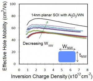
Figure 2: Effective hole mobility as a function of inversion charge density extracted from split C-V and I-V measurements of two similar gate-all-around nanowire MOSFETs with different gate lengths. Increased hole mobility was observed as the NW width is decreased from 75nm down to 15nm.
Figure 1 shows the measured transfer characteristics of ~15nm diameter Gate-all-around nanowire p-MOSFETs with a gate length of 0.75 µm, N=500 parallel NWs, and Al2O3/WN gate stack, demonstrating excellent electrostatics with an on-to-off ratio of more than 1010. Using low-field conductance and split capacitance-voltage measurements of two-MOSFETs with similar series resistance and parasitic capacitances, effective hole mobility and inversion charge density of the NWs were accurately extracted; the results are shown in Figure 2. Monotonic hole mobility increase is observed as the NW width is decreased from ~75nm to ~15nm. The hole mobility increase is attributed to the increased contribution of high-hole mobility (110) sidewalls as well as stress induced by the WN metal gate.
References
- J. Chen, T. Saraya, K. Miyaji, K. Shimizu, and T. Hiramoto, ” Experimental Study of Mobility in [110]- and [100]-Directed Multiple Silicon Nanowire GAA MOSFETs on (100) SOI,” in IEEE VLSI Tech. Dig., pp. 32-33, 2008. [↩]
- O. Gunawan et al., “Measurement of Carrier Mobility in Silicon Nanowire” Nano Letters, vol. 8, no. 6, pp. 1566-1571, Dec. 2008. [↩]