A Novel Platform for Monolithic Integration of III-V Devices with Si CMOS Technology
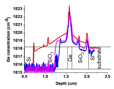
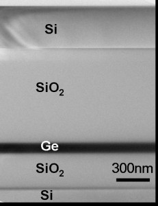
Silicon-on-lattice-engineered-substrates (SOLES), shown in Figure 1, were developed in our group as a substrate platform for integrating III-V devices with Si CMOS technology [1] [2]. The SOLES wafer consists of a Si-on-insulator layer on top of a buried Ge-on-insulator structure. The Ge layer provides a template for III-V growth and device processing [3] [4]. Si CMOS devices can be processed on the SOI layer [4]. Because traditional Si device processing typically involves high temperature steps, the total thermal budget allowed by the SOLES wafer was carefully evaluated. No morphological changes were seen in the SOLES wafers after anneals of up to 915°C. However, Ge agglomeration and film delamination were present in samples annealed at temperatures approaching Ge’s melting point, limiting the allowed thermal budget of the SOLES wafer [5]. A sustained 915°C anneal did result in Ge diffusion, leading to an accumulation of Ge at the Si-SiO2 interfaces (see Figure 2) [5]. This accumulation could lead to deleterious effects on the Si CMOS devices. To date, CMOS device processing with a properly designed thermal budget that limits Ge diffusion has be used to process devices on SOLES [4]. In order to increase the flexibility of the SOLES wafer, a SiNx layer as thin as 250Å can be embedded in the SiO2 in order to block Ge diffusion to the top Si (see Figure 2) [5]. Currently, research is underway toward the next generation of SOLES, including fabrication of low threading dislocation density GaAs-OI and InP-OI. Contact metallurgies to III-V materials that are compatible with Si processing are also being investigated.

Figure 2: SIMS profile of Ge concentration after 8.5h 915°C anneal in SOLES structure (red), in modified structure with 1000Å (blue) and 250Å (pink) of SiNx embedded in the SiO2.
References
- C. L. Dohrman, K. Chilukuri, D. M. Isaacson; M. L. Lee, and E. A. Fitzgerald, “Fabrication of silicon on lattice-engineered substrate (SOLES) as a platform for monolithic integration of CMOS and optoelectronic devices,” Materials Science and Engineering B: Solid-State Materials for Advanced Technology, vol. 135, no.3, pp. 235-237, Dec. 2006. [↩]
- F. Letertre, “Formation of III-V Semiconductor Engineered Substrates Using Smart CutTM Layer Transfer Technology,” in Mater. Res. Soc. Symp. Proc. 2008, vol. 1068, pp. 1068-C01-01. [↩]
- K. Chilukuri, M. J. Mori, C. L. Dohrman, E. A. Fitzgerald, “Monolithic CMOS-compatible AlGaInP visible LED arrays on silicon on lattice-engineered substrates (SOLES),” Semiconductor Science and Technology, vol. 22, pp. 29-34, 2007. [↩]
- W. K. Liu, D. Lubyshev, J. M. Fastenau, Y. Wu, M. T. Bulsara, E. A. Fitzgerald, M. Urteaga, W. Ha, J. Bergman, B. Brar, W. E. Hoke, J. R. LaRoche, K. J. Herrick, T. E. Kazior, D. Clark, D. Smith, R. F. Thompson, C. Drazek, N. Daval, “Monolithic integration of InP-based transistors on Si substrates using MBE,” J. Crystal Growth, vol. 311, no. 7, pp. 1979–1983, Mar. 2009. [↩] [↩] [↩]
- N. Yang, M. T. Bulsara, E. A. Fitzgerald, W.K. Liu, D. Lubyshev, J.M. Fastenau, Y. Wu, M. Urteaga, W. Ha, J. Bergman, B. Brar, C. Drazek, N. Daval, L. Benaissa, E. Augendree W.E. Hoke, J.R. LaRoche, K.J. Herrick, T.E. Kazior, “Thermal Considerations for Advanced SOI Substrates Designed for III-V/Si Heterointegration,” in 2009 IEEE International SOI Conference, pp. 121-122, Oct. 2009. [↩]
