A High-voltage Degradation Mechanism of GaN HEMTs

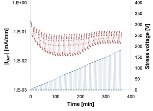
Figure 1: Time evolution of |IGoff| and stress voltage (VDSstress) in a step-stress-recovery experiment in the OFF-state in GaNHEMTs. VDS is step-stressed from 5 V to 180 V in 5 V steps and 5 min stress periods. A 5 min recovery period follows each stress period.
GaN High-Electron-Mobility Transistors (HEMTs) represent a very promising device for high-voltage and high-power RF applications due to the outstanding material properties of GaN such as high band-gap (3.4 eV) and high breakdown electric field (> 3×10⁶ V/cm). This enables GaN HEMTs to achieve a very high breakdown voltage. However, the wide deployment of GaN HEMT technology is mostly limited by its electrical reliability. One of the most prevalent degradation issues in these devices is the crystallographic defect formation through the inverse piezoelectric effect that is believed to take place at high voltage [1]. The high electric field at the drain-side of the AlGaN barrier layer under normal operating conditions induces a large amount of mechanical stress. Above a certain critical value, defects are introduced, which results in electron trapping and subsequent current collapse. Since this degradation is not recoverable, device manufacturers have paid a great deal of attention to mitigating this deleterious mechanism.
Our research focuses on the electrical reliability of GaN HEMTs specially designed for very-high-voltage operation. Our reliability experiments are performed on experimental industrial devices provided by our collaborator, Gal El. These devices are very robust and endure VDG stress voltage up to 200V, which enables us to explore very-high-voltage degradation mechanisms of GaN HEMTs. Our systematic characterization experiments extract important Figures of Merits (FOMs) such as gate leakage current in the OFF state (IGoff), maximum drain current (IDMAX), drain resistance (RD), source resistance (RS) and threshold voltage (VT). These FOMs are continuously measured by a benign characterization suite every minute in the middle of stress tests.

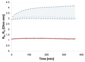
Figure 2: Time evolution of RD and RS in the step-stress-recovery experiment of Figure 1. The full recovery of RD and RS indicates trapping effects that involve only native traps.
Figures 1 and 2 show time evolution of |IGoff|, stress voltage (VDSstress), RD and RS in a step-stress-recovery experiment in the OFF-state at room temperature. A 5 min stress period is followed by a 5 min recovery period under microscope light illumination. For each stress period, VGS = -5 V and constant whereas VDS is incremented from 5 V to 180 V in 5 V step sizes. We find that in these robust devices, IGoff degradation [1] is not observed for VDS stress voltage up to 180 V. IGoff slightly decreases as VDS stress voltage goes up to 100 V and above 100 V, it recovers back to a certain level. |IGoff| and RD (and RS to a much lesser extent) change during the stress periods but recover back to the original level during the recovery periods. These results support a hypothesis in which trapping and detrapping takes place during the stress and recovery periods, respectively, involving only native traps. It also suggests that there is no defect formation up to 180 V of stress voltage. The relatively large change of RD with respect to RS is due to the fact that the field on the drain side is very high, while on the source side it is comparatively small. Moreover, the slight recovery of gate-current depression at a high-stress voltage regime might be due to an additional detrapping mechanism that is under investigation. Since gate-current degradation directly suppresses gain, PAE, and output power in RF power applications, the precise understanding of the impact to high-voltage electrical stress on IGoff is of great importance.
References
- J. Joh and J.A. del Alamo, “Mechanisms for electrical degradation of GaN high-electron mobility transistors,” International Electron Devices Meeting Technical Digest, pp. 415-418, Dec. 2006. [↩]