A Computationally Simple, Wafer-to-feature-scale Model of Etch-rate Variation in Deep Reactive Ion Etching

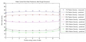
Figure 1: Etch-rate data and model predictions along the middle cross-section of four different, uniformly-patterned wafers.
Modeling etch-rate variation in Deep Reactive Ion Etching (DRIE) helps to identify possible defects in MEMS and IC devices arising from sub-optimal etching depths and times. Besides tool-specific properties, such as the chamber design, another cause for the observed non-uniformity effects is the particular wafer pattern employed, which causes distinctive effects at the wafer-, die-, and feature-scales [1]. We present a model to capture these pattern-dependencies by tracking the spatial and temporal distribution of the ion and radical species within the DRIE chamber. The model implementation uses a time-stepped algorithm with three levels – corresponding to the three different length scales – and a coarse-grained approach whereby multiple features in a given region are characterized by a particular shape, size, and density. The local radical species concentration distribution above the wafer is determined at each time step using current feature geometries to compute their Knudsen transport coefficient, which is linked to the radical transport mechanisms within other areas in the chamber. At the end of each time step, etch-rate estimates based on this radical concentration distribution and current feature geometries are used to update feature depth information for the next time interval. At the wafer scale, our modeling results, shown in part in Figure 1, achieve a success comparable to that of previously-developed wafer-level models with an etch-rate RMS error percentage between 2.1% and 8.2%. The results also show that feature-level etch evolution substantially impacts the wafer-level fluorine concentration and thereby modifies the wafer and die etch-rate uniformity. We expect a similar model could be incorporated into CAD software tools to evaluate masks and correct potential design issues before they are made. Our results also shed light on possible tool and process modifications to allow users the capability of altering across-wafer etch-rate variability.
References
- H. K. Taylor, H. Sun, T. F. Hill, A. Farahanchi, and D. S. Boning, “Characterizing and predicting spatial nonuniformity in the deep reactive ion etching of silicon,” Journal of the Electrochemical Society, vol. 153, pp. C575-C585, 2006. [↩]