High-efficiency Infrared Colloidal Quantum-dot Light-emitting Diodes

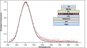
Figure 1: Normalized infrared electroluminescence (black, solid) and photoluminescence (red, crosses) spectra of a PbS QD-LED centered at 1.11 µm. The inset shows the general device structure.

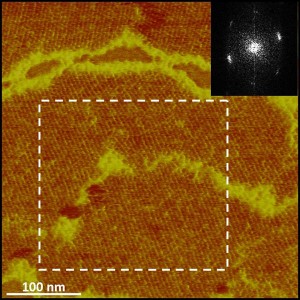
Figure 2: Tapping-mode Atomic Force Microscope (AFM) phase image of nearly complete monolayer coverage of an organic HTL by ~4 nm PbS QDs. QDs have the tendency to pack into regular hexagonal arrays. The inset illustrates a two-dimensional spatial Fourier Transform of the area delineated by the dashed box, revealing the expected six-point pattern.
While boasting high performances and long lifetimes, the associated fabrication and materials costs of established infrared (IR) technologies (such as inorganic light-emitting diodes (LEDs) and lasers) preclude their use in cost-constrained, large-area applications [1]. Solution-processable LEDs promise lower manufacturing costs and compatibility with a variety of (flexible) substrates. In the IR region, the incorporation of solution-processable IR light-emitters into on-chip optoelectronic integrated circuits is an alluring possibility [1]. Optical diagnosis in biologically transparent windows at 800, 1100, and 1300 nm could also be performed using large-area IR emitters [2]. However, solution-processable molecular and polymeric organic LEDs have limited extendibility into the IR region owing to negligible optical activity beyond 1 µm [1]. In contrast, colloidal quantum-dot LEDs (QD-LEDs) combine the thin film processability of organic materials with the tunable optical properties conferred by QD size control. Additionally, the colloidal PbS QDs employed here can be reproducibly synthesized with a narrow size distribution, demonstrate greater stability [3] than PbSe (on which several previously reported devices have been based [1]), and exhibit a remarkably high thin-film absolute photoluminescence (PL) efficiency of 18 to 20 %.
We report efficient IR electroluminescence (EL) from large-area (mm2 in size) LEDs comprising solution-deposited colloidal PbS QDs sandwiched between organic hole- and electron-transporting layers (HTL/ETL) deposited at room temperature, as shown in the inset of Figure 1. Spin-casting of a blend solution of QDs and a hole transporting material yields a QD monolayer at the surface via a spontaneous phase-segregation process previously reported by our group [4] (see Figure 2). IR EL is observed at turn-on voltages as low as 4 V and closely resembles the corresponding QD PL spectrum (Figure 1).
References
- J. S. Steckel, S. Coe-Sullivan, V. Bulović and M. G. Bawendi, “1.3 µm to 1.5 µm Tunable Electroluminescence from PbSe Quantum Dots Embedded within an Organic Device,” Advanced Materials, vol. 15, no. 21, pp. 1862-1866, November 2003. [↩] [↩] [↩] [↩]
- G. Konstantatos, C. Huang, L. Levina, Z. Lu and E. H. Sargent, “Efficient Infrared Electroluminescent Devices Using Solution-Processed Colloidal Quantum Dots,” Advanced Functional Materials, vol. 15, pp. 1865-1869, September 2005. [↩]
- J. Tang, X. Wang, L. Brzozowski, D. A. R. Barkhouse, R. Debnath, L. Levina and E. H. Sargent, “Schottky Quantum Dot Solar Cells Stable in Air under Solar Illumination,” Advanced Materials, vol. 22, pp. 1398-1402, January 2010. [↩]
- S. Coe-Sullivan, J. S. Steckel, W-K. Woo, M. G. Bawendi, V. Bulović, “Large-Area Ordered Quantum-Dot Monolayers via Phase Separation During Spin-Casting,” Advanced Functional Materials, vol. 15, pp. 1117-1124, April 2005. [↩]