Bias Stress Instability in GaN MOSFETs
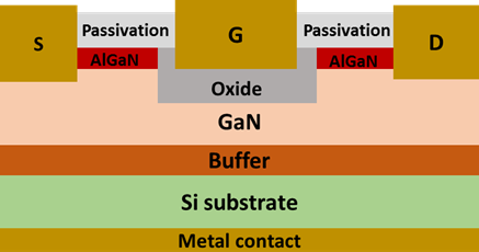
GaN power transistors represent a promising alternative to Si devices for power switching applications. In particular, GaN-high electron mobility transistors with insulated-gate (MIS-HEMTs) have recently attracted much attention because they offer high current, high breakdown voltage and low gate leakage current, all desirable attributes for power transistors. On the other hand, GaN MIS-HEMTs face significant reliability and stability challenges. Among them, the shifting of the threshold voltage after prolonged high voltage stress at elevated temperature is a serious concern. Understanding and proposing solutions to this problem is the goal of this research project.
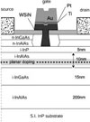
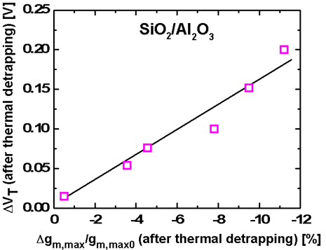
The physical mechanisms responsible for bias stress instability (BTI) in GaN MIS-HEMTs are not well understood because of their complex gate stack structure with multiple interfaces and many trapping sites. In order to isolate the role of the gate oxide and its interface in BTI, we are studying a simpler GaN MOSFET structure in which the gate oxide sits directly on top of the GaN channel. Our research reveals the importance of trapping inside the gate oxide as well as trap state generation at or near the oxide/semiconductor interface. These studies should be instrumental in understanding the more complex instability issues of GaN MIS-HEMTs.
Recent publications:
RC-233 Guo, A. and J. A. del Alamo, Positive-Bias Temperature Instability of GaN MOSFETs. IEEE International Reliability Physics Symposium, Monterey, CA, April 19-23, 2015, pp. 6C.5.1-6C.5.7. (paper) (slides)
|
|