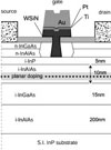
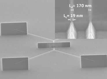
Nanoscale ohmic contacts
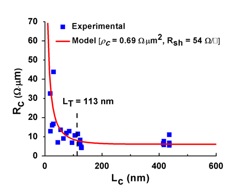
High-performance nano-scale transistors require correspondingly small ohmic contacts with very low contact resistance. It represents a very significant challenge to characterize the electrical characteristics of small contacts for which the metal resistance can become significant. We have proposed and demonstrated a novel test structure to characterize nano-scale metal-semiconductor contacts. We term this the nano-Transmission-Line Model structure or nano-TLM. This is a two-port structure with all dimensions in the nanometer range. Kelvin measurements allow the separate extraction of the metal sheet resistivity, the semiconductor sheet resistance and the contact resistance. We have demonstrated this structure by fabricating Mo nano-contacts to n-type InGaAs heterostructures where we have obtained a record low contact resistance. We have also applied this structure to extract the contact resistance of nano-scale Ni contacts to p-type InGaSb for future p-type MOSFETs. Excellent results were also demonstrated in this case.
Recent publications:
RJ-158 Guo, L. W., W. Lu, B. R. Bennett, J. B. Boos, and J. A. del Alamo, Ultra-low Resistance Ohmic Contacts for p-channel InGaSb Field-Effect Transistors. IEEE Electron Device Letters, Vol. 36, No. 6, pp. 546-548, June 2015.
RJ-146 Lu, W., A. Guo, A. Vardi, and J. A. del Alamo, A Test Structure to Characterize Nano-scale Ohmic Contacts in III-V MOSFETs. IEEE Electron Device Letters, Vol. 35, No. 2, pp. 178-180, February 2014. (paper)
|
|