InGaAs Vertical Nanowire Tunneling FETs (TFETs)
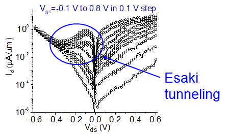
Tunneling Field-Effect Transistors (TFET) based on III-V compound semiconductors are considered a promising approach to implement logic switches that operate at extremely low voltages (~0.3 V). Reduced voltage operation is required to achieve the ultra-high transistor densities needed to maintain progress with Moores Law several generations into the future. The low voltage suitability of TFETs stems from the steep subthreshold characteristics that the tunneling process enables.
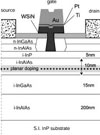
Our group at MIT is investigating InGaAs-based Vertical Nanowire TFETs fabricated by a top-down approach. Towards this goal, we have developed very high aspect ratio dry etching technology of In-containing compound semiconductor heterostructures. This etching approach is flexible and yields thin nanowires with smooth sidewalls. Our TFETs feature and InAs notch to reduce the tunnel barrier height and obtain high ON current. We have demonstrated TFETs with 50 nm nanowire diameter and an ON-OFF ratio that exceeds that of other III-V-based Nanowire TFETs fabricated by more conventional bottom-up techniques.
Recent publications:
RC-231 Zhao, X., A. Vardi and J. A. del Alamo, InGaAs/InAs Heterojunction Vertical Nanowire Tunnel FETs Fabricated by a Top-down Approach. IEEE International Electron Devices Meeting, San Francisco, CA, December 15-17, 2014, pp. 590-593.
RJ-148 Zhao, X. and J. A. del Alamo, Nanometer-scale Vertical-Sidewall Reactive Ion Etching of InGaAs for 3-D III-V MOSFETs. IEEE Electron Device Letters, Vol. 35, No. 5, pp. 521-524, May 2014. (paper)
|
|