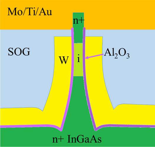
InGaAs Vertical Nanowire MOSFETs
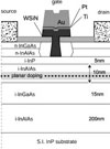
The vertical nanowire (VNW) MOSFET represents the ultimate scalable transistor. The gate-all-around nanowire configuration allows for the highest degree of charge control in the channel. The vertical transport direction uncouples footprint scaling (on the plane of the wafer) from gate length scaling (normal to the wafer) leading to the best possible combination of transistor density and short-channel effects. At MIT, we are investigating vertical nanowire InGaAs MOSFETs fabricated by an innovative top-down approach. Towards this goal, we have developed Reactive Ion Etching technology to etch In-containing III-V compounds that yields high aspect ratio structures with vertical and smooth sidewalls. We have also developed a new digital etch technique to controllably thin down nanowires and further smooth the sidewalls without any changes in the aspect ratio. Using this technology, we have demonstrated InGaAs VNW MOSFETs with nanowire diameters as thin as 30 nm. We have obtained performance in terms of transconductance vs. short-channel effects that is comparable with better established bottom-up approaches.
Recent publications:
RJ-148 Zhao, X. and J. A. del Alamo, "Nanometer-scale Vertical-Sidewall Reactive Ion Etching of InGaAs for 3-D III-V MOSFETs." IEEE Electron Device Letters, Vol. 35, No. 4, pp. 521-523, May 2014. (paper)
RJ-147 Lin, J., X. Zhao, D. A. Antoniadis, and J. A. del Alamo, "A Novel Digital Etch Technique for Deeply Scaled III-V MOSFETs." IEEE Electron Device Letters, Vol. 35, No. 4, pp. 440-442, April 2014. (paper)
RC-220 Zhao, X., J. Lin, C. Heidelberger, E. A. Fitzgerald and J. A. del Alamo, "Vertical Nanowire InGaAs MOSFETs Fabricated by a Top-down Approach." IEEE International Electron Devices Meeting, Washington DC, December 9-11, 2013, pp. 695-698. (paper) (slides)
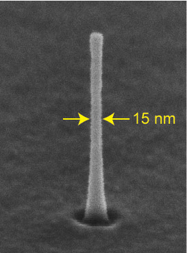
15 nm diameter, vertical InGaAs nanowire fabricated by reactive ion etching and digital etch. This is the core of vertical InGaAs nanowire MOSFETs fabricated by Xin Zhao. Learn more here |
|