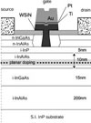
InGaAs FinFETs
In our quest to exploit the extraordinary electron transport properties of InGaAs, we are investigating three-dimensional transistor architectures. Among them, the FinFET exhibits outstanding potential to scale to sub 10-nm dimensions. In a FinFET, the channel is placed normal to the wafer surface (hence the name fin) and the gate modulates the carrier concentration from both sides. This provides outstanding charge control capabilities, great immunity to short-channel effects and an ability to scale to very small dimensions.
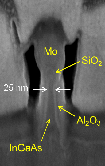
At MIT, we are investigating critical issues required for a future high-performance InGaAs FinFET technology. Towards this goal, we have developed a new deep reactive ion etching technology to form high aspect ratio fins on III-V heterostructures that include In-containing III-V compounds. We have also innovated a new digital etch technique that allows us to smooth the etched the sidewalls while preserving the high-aspect ratio. We have also developed a novel contact-first approach for InGaAs FinFETs that yields unprecedented low contact resistance. These technologies have allowed us to fabricate InGaAs FinFETs with fin widths as narrow as 12 nm. In these devices, we have shown that the interface state density at the sidewalls is comparable to that of planar surfaces. This demonstrate the grate potential of our approach.
Recent publications:
RJ-156 Vardi, A., W. Lu, X. Zhao and J. A. del Alamo, "Nano-scale Mo Ohmic Contacts to III-V Fins." IEEE Electron Device Letters, Vol. 36, No. 2, pp. 126-128, February 2015. (paper)
RC-224 Vardi, A., X. Zhao, and J. A. del Alamo, "InGaAs Double-Gate Fin-Sidewall MOSFETs." 72nd IEEE Device Research Conference, Santa Barbara, CA, June 22-25, 2014.
RJ-148 Zhao, X. and J. A. del Alamo, "Nanometer-scale Vertical-Sidewall Reactive Ion Etching of InGaAs for 3-D III-V MOSFETs." IEEE Electron Device Letters, Vol. 35, No. 4, pp. 521-523, May 2014. (paper)
RJ-147 Lin, J., X. Zhao, D. A. Antoniadis, and J. A. del Alamo, "A Novel Digital Etch Technique for Deeply Scaled III-V MOSFETs." IEEE Electron Device Letters, Vol. 35, No. 4, pp. 440-442, April 2014. (paper)
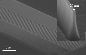
InGaAs fin array and 20 nm wide fin (inset) |
|