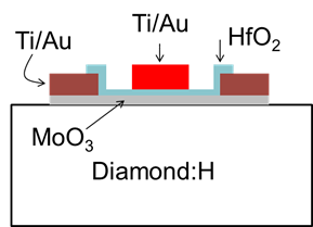
Diamond MOSFETs
Diamond is widely considered the ultimate semiconductor for the realization of solid-state microelectronics devices. This is due to its outstanding mechanical, electrical and thermal properties, such as extreme hardness, high breakdown electric field, very high thermal conductivity and high intrinsic carrier mobilities at room temperature. Progress in the realization of diamond-based electronic devices has been hampered by the lack of suitable dopants with low activation energies. This drawback has been partially overcome through surface transfer doping or the creation of a highly conductive sheet of holes at the diamond subsurface when hydrogen-terminated diamond (Diamond:H) is exposed to surface acceptors with high work function. The surface transfer doping system that has been most studied consists of Diamond:H exposed to H2O molecules. A major difficulty of this is the gradual desorption of H2O that takes place at even moderate temperatures. This poses severe constraints on the process technology as well as the reliability of transistors fabricated in this system.
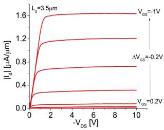
Recently, MoO3 has been shown to exhibit excellent transfer doping properties with Diamond:H, yielding the highest yet reported areal hole density and showing temperature stability up to at least 350°C. In this project we are investigating Diamond:H/MoO3 transfer-doped MOSFETs. We have recently achieved the first working MOSFETs in this material system. While the performance is modest, opportunities for substantial device improvement clearly exist.
Recent publications:
RJ-153 Vardi, A., M. Tordjman, J. A. del Alamo and R. Kalish, A Diamond:H/MoO3 MOSFET. IEEE Electron Device Letters, Vol. 35, No. 12, pp. 1320-1322, December 2014. (paper)
|
|