Low-voltage SRAM Caches with On-fly Energy Monitoring for Exascale Processors
On-chip memories are responsible for a large portion (40% by many estimates [1] ) of the total energy consumption and area of modern processor designs. A 50-MB on-chip cache has been reported [2] . Larger memories integrated into systems in scaled technologies make low-power memory design a very important research topic.
The static-noise-margin (SNM) is the conventional way to quantify the stability of a bit-cell. Read and write SNM are used for analyzing read and write problems, respectively; hold SNM gives the margin for retention as shown in Figure 1(b). A conventional 6-transistor (6T) SRAM cell fails to operate at low voltage levels due to increased effect of variation. In order to address the read SNM problem of a 6T bit-cell, two extra transistors can be inserted into the cell, forming the read-buffer [3] . This 8-transistor (8T) bit-cell is given in Figure 1(d). In this bit-cell, read and write ports are de-coupled, and transistor sizing can be done independently to favor both read and write functions. This way, the SRAMs can be designed to work down to their retention voltages. For an 8k-bit SRAM block (64 columns and 128 rows), memory error maps are simulated as given in Figure 1(a) at 250mV. In order to achieve ultra low-voltage operation, the 8T bit-cell with write-assist circuits has been selected for our design. The extra two transistors result in a ~30% area increase. However, voltage scaling from 1.2V down to 0.4V would result in an almost ~10x reduction in energy per operation.
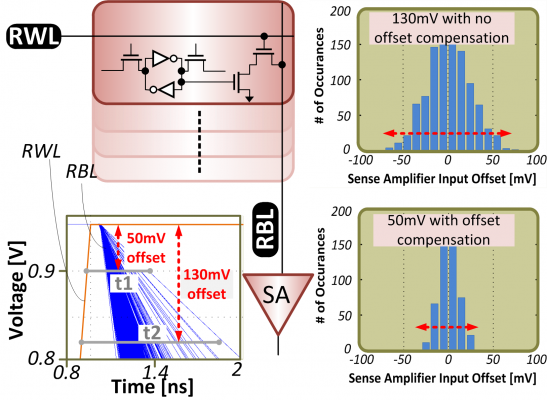
For the 8T bit-cell, a single-ended sense amplifier (SA) is necessary since the read-bit-line (RBL) is the only port used for reading. The offset of SA is reduced using offset-compensation techniques, and this concept is illustrated by 1000-point Monte Carlo analyses on input offset of our strong-arm type SA with or without compensation.
-
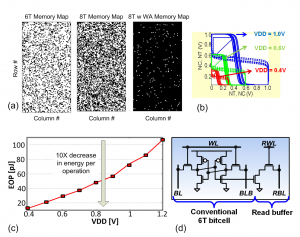
- Figure 1: (a) Simulated memory maps for an 8k-bit memory at 250mV show that 8T with WA has fewer errors (b) The side length of the largest square that can fit inside the lobes of a butterfly curve gives the hold margin. (c) Measured energy per operation per bit decreases by ~10X by voltage scaling from 1.2V to 0.4V (d) 8T bit-cell

-
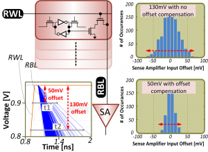
- Figure 2: Access time is limited by the worst-case bit-cell’s discharge time of the RBL by the worst-case SA offset. Decreasing input offset from 130mV to 50mV results in almost 2 times less discharge time for the worst-case bit-cell.
- N. Ickes, Y. Sinangil, F. Pappalardo, E. Guidetti, A. P. Chandrakasan ; “A 10 pJ/cycle ultra-low-voltage 32-bit microprocessor system-on-chip,” ESSCIRC, pp.159-162, 12-16 Sept. 2011. [↩]
- R. J. Riedlinger, R. Bhatia, L. Biro, B. Bowhill, E. Fetzer, P. Gronowski, T. Grutkowski, “A 32nm 3.1 billion transistor 12-wide-issue Itanium® processor for mission-critical servers,” ISSCC, pp.84-86, 20-24 Feb. 2011. [↩]
- N. Verma and A. P. Chandrakasan, “A 65nm 8T Sub-Vt SRAM Employing Sense-Amplifier Redundancy,” ISSCC, pp.328-606, 11-15 Feb. 2007. [↩]