- Authors: P. R. Brown, N. Zhao, R. R. Lunt, J. Jean, T. P. Osedach, M. G. Bawendi, V. Bulović
- Sponsorship: Hertz Foundation, National Science Foundation, Samsung
Solar cells based on lead sulfide quantum dots (PbS QDs) represent a promising new class of solution-processable photovoltaics. The highly tunable bandgap of PbS QDs (0.5-2.1 eV) makes them ideally suited for incorporation into multijunction architectures, and their resistance to oxidation and photobleaching represent further advantages over typical solution-processed photovoltaic materials such as organic small molecules and polymers [] [] .
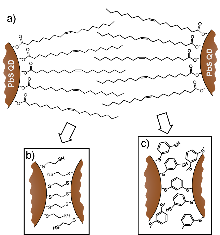
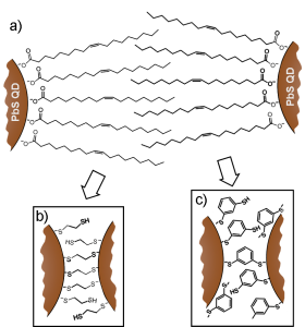
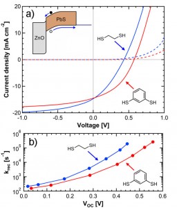
The electronic properties of QD films are determined not only by the size and composition of the QDs themselves but also by the properties of the organic ligands used to passivate the QD surfaces. As-synthesized PbS QDs are stabilized in solution by long, insulating oleic acid ligands, which are unsuitable for use in photovoltaics, where efficient electron transport is required. Therefore, a ligand-exchange treatment is typically performed, replacing the oleic acid ligands with short, bidentate molecules such as 1,2-ethanedithiol (EDT). Our research demonstrates that the power conversion efficiency of ZnO/PbS QD heterojunction photovoltaics [] may be enhanced through ligand exchange with 1,3-benzenedithiol (BDT) rather than the more common EDT, despite the fact that BDT-treated films demonstrate a lower charge carrier mobility than EDT-treated films. Treatment with BDT simultaneously increases the fill factor (FF) and open-circuit voltage (VOC) relative to treatment with EDT, thereby increasing the power conversion efficiency by a factor of 1.6, from 2.1% to 3.4%. Measurement of the transient photovoltage response of the devices indicates that this increase in FF and VOC results from a decrease in the rate of bimolecular recombination and the concomitant increase in carrier lifetime within the QD film. This increase in carrier lifetime more than compensates for the lower mobility of BDT-treated films, emphasizing the importance of designing ligands that simultaneously decrease the inter-QD spacing and effectively passivate surface recombination sites.
-
-
Figure 1: Schematic representation of lead sulfide quantum dots with a) oleic acid ligands. Following ligand exchange, the oleic acid ligands are replaced with b) 1,2-ethanedithiol (EDT) or c) 1,3-benzenedithiol (BDT).
-
-
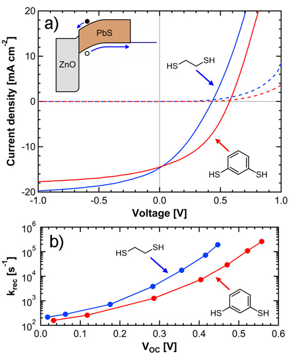
Figure 2: a) Current-voltage characteristics of a ZnO/PbS QD heterojunction photovoltaic device, where ligand exchange has been performed with EDT (blue trace) or BDT (red trace). BDT treatment simultaneously increases the fill factor, open-circuit voltage, and efficiency. b) Transient photovoltage response of the device, demonstrating a reduced recombination rate (krec) for BDT-treated devices relative to EDT-treated devices.
- Authors: J. Jean, S. Chang, P. R. Brown, J. W. J. Cheng, P. Rekemeyer, M. G. Bawendi, S. Gradečak, V. Bulović
- Sponsorship: MIT Energy Initiative
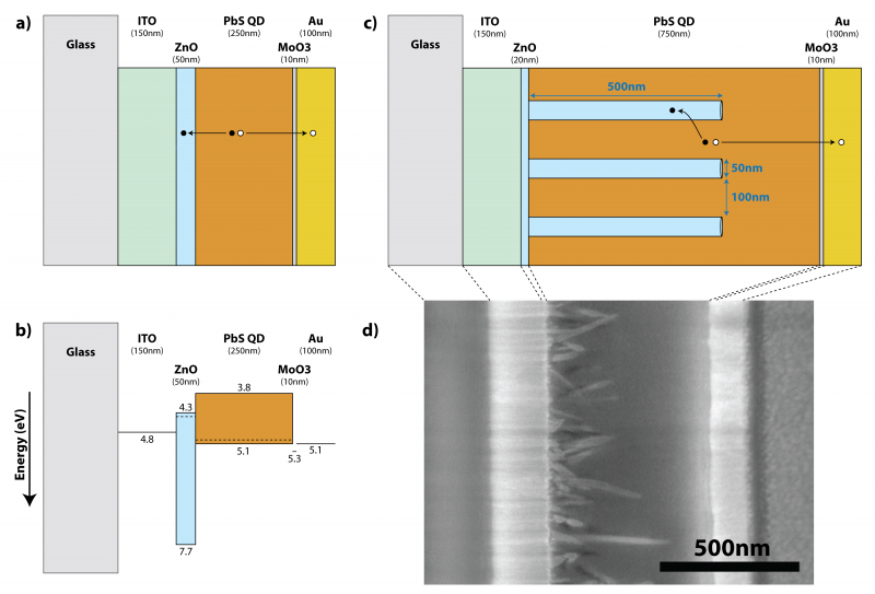
Thin-film solar cells incorporating colloidal quantum dot active layers have recently emerged as a notable third-generation photovoltaic (PV) technology, largely due to the strong absorption, tunable infrared bandgap, and ambient-atmosphere stability of lead sulfide quantum dots (PbS QDs). Photoactive PbS QDs can be solution-deposited on a transparent zinc oxide (ZnO) film to form a depleted np-heterojunction device (Figure 1a,b). However, this standard planar architecture incurs a fundamental trade-off between light absorption and carrier collection: to absorb most incident light, we need a ~1-µm-thick QD film [] , but to collect most photocarriers, we need absorption to occur within a minority carrier diffusion length (~100 nm) of the ~150-nm-thick depletion region [] . By introducing 1-D nanostructures (Figure 1c), we can decouple these parallel requirements and optimize for each independently. A vertical, QD-infiltrated array of ZnO nanowires orthogonalizes the mechanistic length scales of absorption and collection. Absorption is maximized as light traverses a thick QD film in the axial direction, while field-driven carrier collection is retained throughout the film as photogenerated electrons drift to nearby PbS/ZnO interfaces in the radial direction.
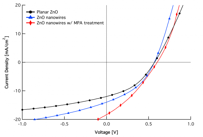
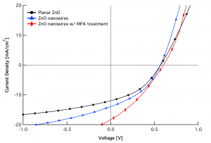
Our research demonstrates that moving from a planar ZnO film to a nanowire array can significantly improve QDPV performance, increasing short-circuit current density (JSC) by ~40% and overall power conversion efficiency by ~15% [] . We confirm the near-complete infiltration of PbS QDs into the ZnO nanowire array via cross-sectional scanning electron microscopy (Figure 1d) and elemental mapping with energy-dispersive x-ray spectroscopy. We further demonstrate a fast solution treatment to assist interfacial charge transfer using a bifunctional linker molecule, 3-mercaptopropionic acid (MPA). A simple MPA treatment increases both JSC and open-circuit voltage (VOC) of nanowire-QD devices (see Figure 2). Our work on ZnO nanowire-based QD solar cells—along with the recent demonstration of a 5.6%-efficient TiO2nanopillar-based QDPV [] —suggests that 1-D nanostructures may be the key to enhancing the efficiency and hence the economic viability of quantum dot photovoltaics.
-

-
Figure 1: (a) Schematic and (b) energy band diagram of a standard planar quantum dot photovoltaic (QDPV) device with parallel light absorption and carrier collection pathways. A modified architecture incorporating ZnO nanowires—shown here by (c) schematic and (d) cross-sectional scanning electron micrograph—decouples absorption from collection and extends the effective depletion width throughout a QD film of arbitrary thickness.
-
-
Figure 2: J-V characteristics (under AM1.5G illumination) of planar (black circles) and nanowire QDPV devices fabricated in a single run. Incorporation of ZnO nanowires (blue triangles) boosts the short-circuit current density (JSC) without affecting the open-circuit voltage (VOC). An additional interface treatment with 3-mercaptopropionic acid (MPA) (red diamonds) concurrently increases JSC, VOC, and overall power conversion efficiency of the nanowire-based devices.
- Authors: A. Maurano, D.-K. Ko, P. Brown, J. Jean, V. Bulović
- Sponsorship: ENI-MIT Solar Frontier Center
Colloidal lead sulfide quantum dot (PbS QD) solar cells have recently shown attractive improvements in efficiency [1]. PbS QDs have been investigated in various device architectures—including Schottky junction, depleted planar heterojunction, and ordered bulk heterojunction photovoltaic (PV) architectures—with the aim of maximizing light absorption while maintaining efficient charge transport [] . However, the thickness of the PbS QD layer in the aforementioned architectures remains limited by the relatively short exciton diffusion length characteristic of all QD films. We developed a novel architecture in which PbS QDs and zinc oxide (ZnO) nanoparticles are co-deposited from solution to form a bulk heterojunction (BHJ). Much like a typical polymer BHJ solar cell, these PbS QD PV devices can decouple the light absorption, which is proportional to device thickness, from the exciton diffusion length [] . We fabricated these BHJ PbS QD:ZnO solar cells in solution by layer-by-layer deposition in which each step is followed by ligand exchange as shown in Figure 1a. By conducting preliminary optimization of the processing condition, we obtained the current density as a function of the applied voltage graph shown in Figure 1b. Further studies aim at improving device performance while studying the morphological conformation of PbS and ZnO domains.

Figure 1: a) Schematic of the solution process for fabrication of bulk heterojunction lead sulfide quantum dots (PbS QD) and zinc oxide (ZnO) solar cells. The devices are fabricated by layer-by-layer deposition in which each step is followed by ligand exchange. b) JV characteristics under dark (squares) and AM 1.5 illumination (circles) for planar (control – red) and bulk heterojunction (blue) PbS QD:ZnO devices.
- Authors: H. Park, P. R. Brown, V. Bulović, J. Kong
- Sponsorship: Eni S.p.A, Fannie and John Hertz Foundation, NSF
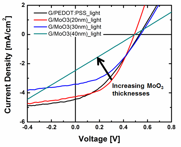
Due to the remarkable physical properties of graphene, applications in various areas such as transistors [] , chemical sensors [] , and logic devices [] have been explored; a variety of proof-of-concept devices have been demonstrated. In this work, organic photovoltaics (OPV) with graphene electrodes are constructed so that the effects of graphene morphology (Figure 1), hole transporting layers (HTL) (Figure 2), and counter electrodes are presented. One of the challenges in the integration of graphene in OPV is the incompatibility between the graphene electrode and poly(3,4-ethylenedioxythiophene):poly(styrenesulfonate) (PEDOT:PSS) hole transport layer (HTL) which significantly increases the device failure rate [] . When hydrophilic PEDOT:PSS is spin-coated onto graphene, it is difficult to achieve uniform and conformal coating due to the hydrophobic nature of the graphene surface, i.e., lower surface free energy. Instead of the conventional PEDOT:PSS HTL, an alternative transition metal oxide HTL (molybdenum oxide (MoO3)) is investigated to address the issue of surface immiscibility between graphene and PEDOT:PSS. The graphene films considered here are synthesized via low-pressure chemical vapor deposition (LPCVD) using a copper catalyst, and experimental issues concerning the transfer of synthesized graphene onto the substrates of OPV are discussed. The morphology of the graphene electrode and HTL wettability on the graphene surface are shown to play important roles in the successful integration of graphene films into the OPV devices. The effect of various cathodes on the device performance is also studied. These factors (i.e., suitable HTL, graphene surface morphology and residues, and the choice of well-matching counter electrodes) will provide better understanding for utilizing graphene films as transparent conducting electrodes in future solar cell applications.
-
-
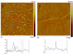
Figure 1: AFM images of graphene morphology of different numbers of layers: (A) 3 layers and (B) 1 layer. Cross-sectional profiles of dotted regions are shown below. Much denser concentration of wrinkles on 3-layered graphene films are observed compared to a single-layer graphene sheet. The surface of stacked layers is thus much rougher than the single-layer sheet with a rms roughness more than 3-fold higher: 2.0 nm for 3 layers and 0.6 nm for 1 layer.
-

-
Figure 2: Current density vs. voltage characteristics of graphene OPV devices with PEDOT:PSS and MoO3 hole transporting layers with varying MoO3 HTL thicknesses (20-40 nm) under simulated AM 1.5G illumination at 100 mW/cm2. By utilizing the thermally evaporated MoO3 HTL, the wetting of HTL on graphene surface can be improved compared to the conventional PEDOT:PSS HTL.