Hot Carrier-Assisted Intrinsic Photoresponse in Graphene
The photoresponse of semiconductors, which determines the performance of optoelectronic devices, is governed by energy relaxation pathways of photoexcited electron-hole (e-h) pairs: energy transferred to the lattice is lost as heat while energy transported through charge carriers may be used to drive an optoelectronic circuit [1] . In graphene, energy relaxation pathways are strongly altered by the vanishing electronic density of states. After initial relaxation of photo-excited carriers caused by electron-electron scattering and optical phonon emission, electron-lattice energy relaxation can be quenched [2] , resulting in a novel transport regime in which thermal energy is redistributed solely among electronic charge carriers.
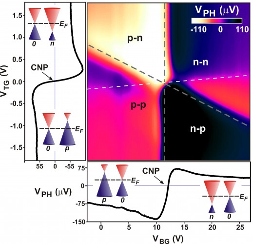
While graphene is considered an excellent candidate for photodetection and energy-harvesting applications due to its broadband optical response and high internal quantum efficiency, measurements have not clearly determined the photocurrent generation mechanism. Here, we report on the intrinsic photoresponse of dual-gated monolayer and bilayer graphene p-n junction devices (Figure 1). Local laser excitation of wavelength 850 nm at the p-n interface leads to striking six-fold photovoltage patterns as a function of bottom- and top-gate voltages (Figure 2). These patterns, together with the measured spatial and density dependence of the photoresponse, provide strong evidence that non-local hot carrier transport, rather than the photovoltaic effect, dominates the intrinsic photoresponse in graphene [3] [4] . The hot carrier regime manifests as a strong photo-thermoelectric effect in which the photogenerated carrier population remains hot while the lattice stays cool.
-

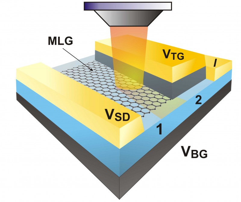
- Figure 1: Experimental schematic image of the dual-gated graphene photodetector device incorporating boron nitride (BN) top gate dielectric and monolayer graphene (MLG). The current I is measured at fixed bias voltage VSD while the top- and bottom-gate voltages, VTG and VBG, respectively, are varied.
-

- Figure 2: Photovoltage vs. VBG and VTG at T=40 K (measured at the center of the device). Gray dashed lines are lines of high resistance from transport characteristics. Also shown are photovoltage line traces taken along the vertical (left) and diagonal (bottom) gray lines.
- S. M. Sze, Physics of Semiconductor Devices, 2nd ed., London: Wiley, Dec. 1981. [↩]
- R. Bistritzer and A. H. MacDonald, “Electronic cooling in graphene,” Physical Review Letters, vol. 102, p. 206410, May 2009. [↩]
- N. M. Gabor, J. C. W. Song, Q. Ma, N. Nair, T. Taychatanapat, K. Watanabe, T. Taniguchi, L. S. Levitov, and P. Jarillo-Herrero, “Hot carrier-assisted intrinsic photoresponse in graphene,” Science, vol. 334, pp. 648-652, Oct. 2011. [↩]
- J. C. W. Song, M. S. Rudner, C. M. Marcus, and L. S. Levitov, “Hot carrier transport and photoresponse in graphene,” Nano Letters, vol. 11, pp. 4688-4692, Sep. 2011. [↩]