Graphene as Transparent Conducting Electrodes in Organic Photovoltaics: Studies in Graphene Morphology, Hole Transporting Layers, and Counter Electrodes
Due to the remarkable physical properties of graphene, applications in various areas such as transistors [1] , chemical sensors [2] , and logic devices [3] have been explored; a variety of proof-of-concept devices have been demonstrated. In this work, organic photovoltaics (OPV) with graphene electrodes are constructed so that the effects of graphene morphology (Figure 1), hole transporting layers (HTL) (Figure 2), and counter electrodes are presented. One of the challenges in the integration of graphene in OPV is the incompatibility between the graphene electrode and poly(3,4-ethylenedioxythiophene):poly(styrenesulfonate) (PEDOT:PSS) hole transport layer (HTL) which significantly increases the device failure rate [4] . When hydrophilic PEDOT:PSS is spin-coated onto graphene, it is difficult to achieve uniform and conformal coating due to the hydrophobic nature of the graphene surface, i.e., lower surface free energy. Instead of the conventional PEDOT:PSS HTL, an alternative transition metal oxide HTL (molybdenum oxide (MoO3)) is investigated to address the issue of surface immiscibility between graphene and PEDOT:PSS. The graphene films considered here are synthesized via low-pressure chemical vapor deposition (LPCVD) using a copper catalyst, and experimental issues concerning the transfer of synthesized graphene onto the substrates of OPV are discussed. The morphology of the graphene electrode and HTL wettability on the graphene surface are shown to play important roles in the successful integration of graphene films into the OPV devices. The effect of various cathodes on the device performance is also studied. These factors (i.e., suitable HTL, graphene surface morphology and residues, and the choice of well-matching counter electrodes) will provide better understanding for utilizing graphene films as transparent conducting electrodes in future solar cell applications.
-
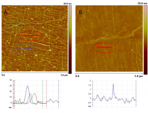
- Figure 1: AFM images of graphene morphology of different numbers of layers: (A) 3 layers and (B) 1 layer. Cross-sectional profiles of dotted regions are shown below. Much denser concentration of wrinkles on 3-layered graphene films are observed compared to a single-layer graphene sheet. The surface of stacked layers is thus much rougher than the single-layer sheet with a rms roughness more than 3-fold higher: 2.0 nm for 3 layers and 0.6 nm for 1 layer.

-

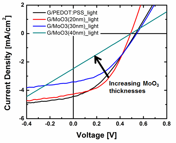
- Figure 2: Current density vs. voltage characteristics of graphene OPV devices with PEDOT:PSS and MoO3 hole transporting layers with varying MoO3 HTL thicknesses (20-40 nm) under simulated AM 1.5G illumination at 100 mW/cm2. By utilizing the thermally evaporated MoO3 HTL, the wetting of HTL on graphene surface can be improved compared to the conventional PEDOT:PSS HTL.
- Y. M. Lin, K. A. Jenkins, A. Valdes-Garcia, J. P. Small, D. B. Farmer, and P. Avouris, “Operation of graphene transistors at gigahertz Frequencies,” Nano Letters, vol. 9, no. 1, pp. 422-426, 2009. [↩]
- P. K. Ang, W. Chen, A. T. S. Wee, and K. P. Loh “Solution-gated epitaxial graphene as pH sensor,” Journal of the American Chemical Society, vol. 130, no. 44, pp. 14392-14393, 2008. [↩]
- R. Sordan, F. Traversi, and V. Russo, “Logic gates with a single graphene transistor,” Applied Physics Letters, vol. 94, no. 7, p. 073305, 2009. [↩]
- H. Park, J. A. Rowehl, K. K. Kim, V. Bulović, and J. Kong, “Doped graphene electrodes for organic solar cells,” Nanotechnology, vol. 21, no. 50, p. 505204, 2010. [↩]